PCB Design Service
Our PCB Design Capabilities
From circuit board layout to schematic designs, we offer PCB design services to meet your product development needs. With our team of experienced engineers, you can be sure that your product design is in good hands. We leverage the latest technology and industry best practices to deliver quality results within the agreed upon schedule.
PCB design and layout
You can outsource your PCB design to us. Our in-house engineers can help you create the perfect PCB for your project. We can fulfill your PCB design requirements using different software like Altium Designer and KiCAD.
PCB stack-up design
We can design and manufacture your PCBs with a particular stack-up to suit your application. We can also incorporate resistors, capacitors, and other passive components onto your PCB to achieve the desired functionality.
Schematic capture
Our schematic engineers work with both AutoCAD and Eagle schematic software. We provide you with a comprehensive report at the end of the project that includes all of the schematics, a bill of materials and the electrical design.
3D modelling
We provide high-quality 3D models for your PCB projects. High accuracy, resolution and detail are guaranteed. You can get your 3D model in STL or VRML format.
PCB reverse engineering
This service is suitable for those who want to create a new version of an existing PCB by extracting detailed electrical data from it. With this data, you can create a new PCB or reproduce an existing one.
Signal integrity services
The integrity of the signal is critical for systems that operate with very low margin for error, like medical or aerospace applications. We can assist you with meeting any signal integrity requirements on your high speed boards.
From schematic design to final production, we provide you with every stage of the manufacturing process. We have expertise in pcb design for various industries, such as medical devices, military, industrial equipment, and others. Our Full electronic design capabilities start to finish including:
- Micro bga stencil design
- PCB Thermal design optimization
- Component Library Development
- PCB layout for high-density modular
- Radio frequency (RF) design
- High speed up tp 56G-PAM4
- Through holes optimal layout
- Digital vs. analog board design
- Minimum BGA PIN Pitch 0.3mm
- DFM/DFA layout validation
- Electromagnetic interference (EMI) checking
- Database Construction and Verification
- Signal integrity and crosstalk reduction
- Routing and impedance control
PCB Design Softwares
We conduct a thorough pcb design review to suggest the most appropriate pcb software for the job. We then work with you to develop the necessary schematics and blueprints before generating the final pcb manufacturing process. (In this post, we have created a list of 46 popular PCB design programs. )
- Altium Designer
- DipTrace
- KiCad EDA
- Cadence Allegro
- OrCAD
- Autodesk
PCB Design Process
There are many steps involved in the PCB design process, from initial planning and schematic creation to layout and routing. Here is a brief overview of the main steps:
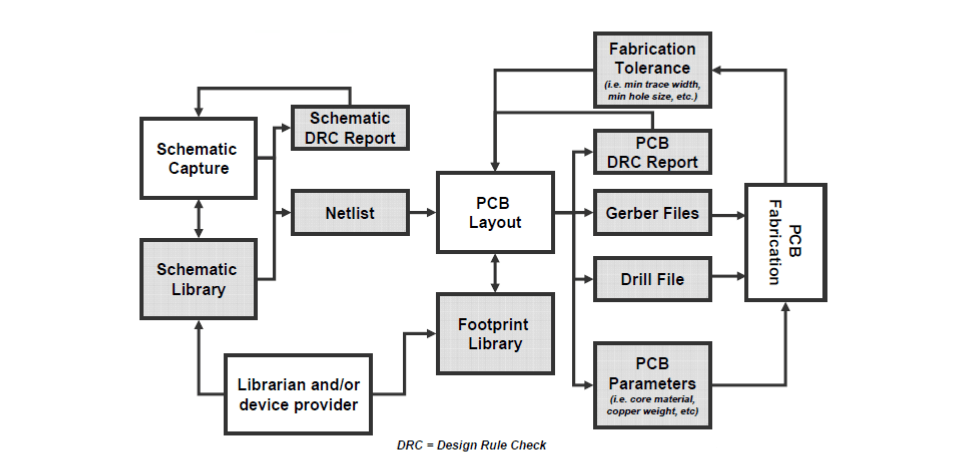
1. Initial Planning
In this stage, you will need to define the circuit requirements and specifications inlcuding the overall size, shape, and purpose of the PCB.
2. Create a Schematic Diagram
There are many ways to create a schematic diagram, but the general process is fairly similar regardless of the software you use:
First, you’ll need to choose a PCB design software. There are many different schematic capture program available, such as Eagle, Altium Designer, Autodesk EAGLE or KiCad. It’s important to choose one that’s compatible with your operating system and has the features you need.
Second, once you’ve chosen a software program, you’ll need to create a new project and add your components to the schematic. To do this, you’ll need to know the footprint and pinout for each component.
Third, once you’ve added all of your components, you’ll need to connect them together with wires.
Forth, you’ll need to add labels to the wires so that you can easily identify them later.
Finally, you can save your schematic now and generate a Gerber file.
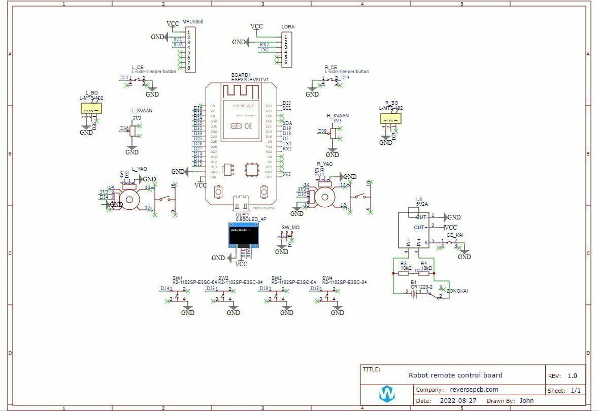
There are a few things to keep in mind when creating a PCB schematic diagram:
- Make sure all of the components are clearly labelled. This includes their names and values (if applicable).
- Draw the diagram to scale. This will make it easier to transfer the design to the PCB layout later on.
- Use standardised symbols for the components. This will make the diagram easier to read and understand.
- Keep the diagram as simple as possible. Avoid unnecessary clutter which could make the design more difficult to transfer to the PCB layout.
- Make sure the diagram is neat and tidy. This will again help with the transfer to the PCB layout stage.
3. PCB Layout
Once the schematic is complete, it’s time to start laying out the PCB. This involves placing all the components onto the board and routing the connections between them. When you lay out the PCB, you should refer to the schematic and try to meet the following requirements:
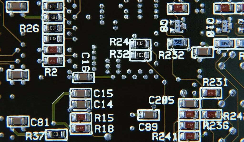
Decoupling capacitor
A decoupling capacitor should be added between the power input pin of each integrated circuit and the ground. The decoupling capacitor should be as close as possible to the power supply pin of the IC, and the loop formed between it and the power supply and the ground should be the shortest.
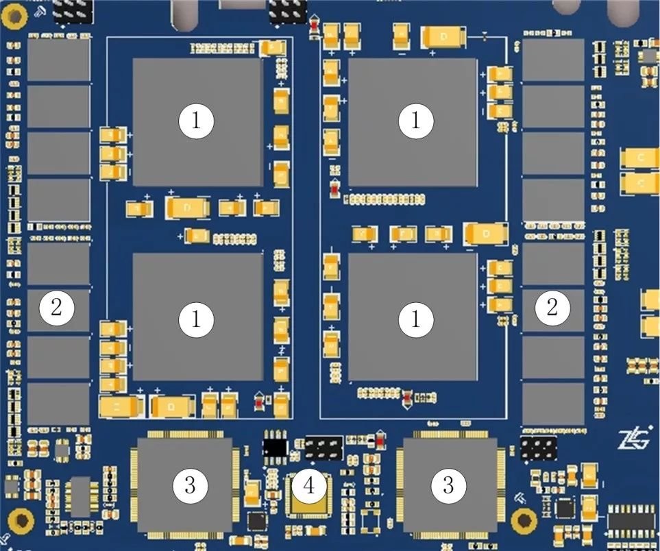
Large vs Small Components
The arrangement of components should be convenient for debugging and maintenance. In another word, the large components cannot be placed around small components, and there should be enough space around components to be debugged.
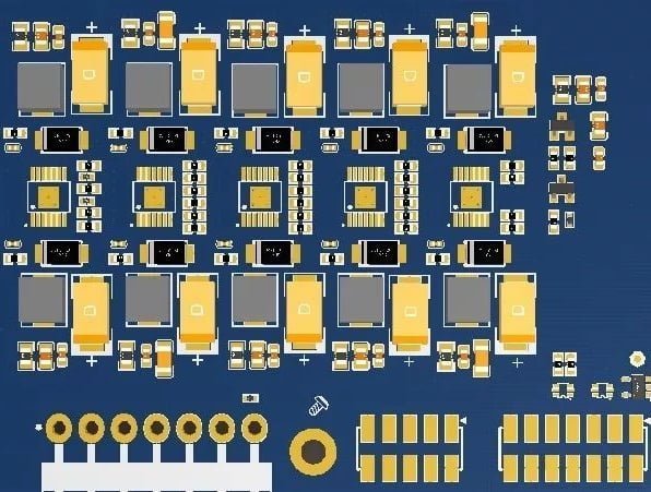
circuit with same structure
For the circuit parts of the same structure, the "symmetrical" standard layout should be adopted as much as possible, and the connections between components and functional blocks should be adjusted for simplicity.
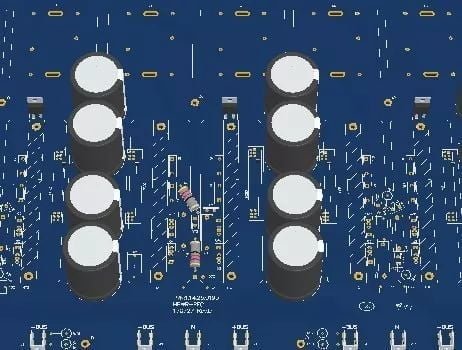
Plug-in components
Plug-in components of the same type should be placed in one direction in the X or Y direction. The same type of polarized discrete components should also be consistent in the X or Y direction, which is convenient for production and inspection.
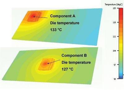
heating components
The heating elements should be evenly distributed to facilitate the heat dissipation of the single board and the whole machine. And the heating element should be placed separately from the temperature sensitive element (except the temperature detection element).
power components
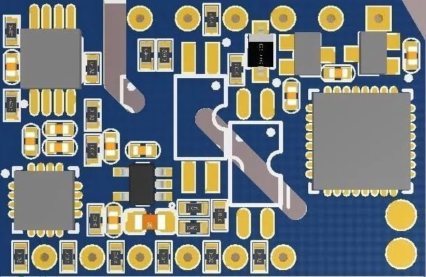
When laying out components, due consideration should be given to placing devices using the same power supply as close as possible to facilitate future power supply separation.
4. PCB Routing
Routing is the process of connecting the various components on the PCB. It is the most important process in the entire PCB design. This will directly affect the performance of the PCB board. Below are top 10 PCB Routing Tips for you:
Use vias to connect different layers of the PCB;
Use different widths for different traces;
Don't Use 90 Degree trace angles;
Use copper pour areas to reduce resistance;
Make sure traces are well-isolated from each other to avoid crosstalk;
Place power and ground traces on separate layers to minimize noise;
Use the ground plane to reduce noise and improve signal integrity;
Route the power and ground lines first, followed by the signal lines;
Keep the trace widths and spacing consistent to avoid signal crosstalk;
Use the shortest possible trace length to reduce signal degradation.
5. Testing and Manufacturing
Once the PCB is complete, it will need to be tested to ensure that it works as intended. After that, it can be sent off to a manufacturer for mass production.
Useful PCB Test Tools
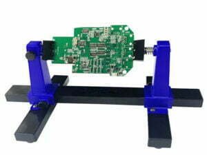
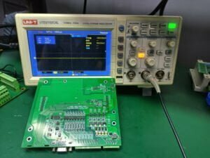
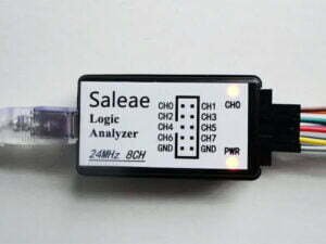
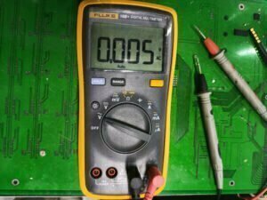
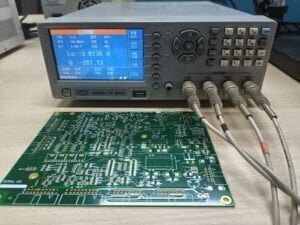
There are many tools that can be used to test a printed circuit board design. One of the most important aspects of testing a custom PCB design is to ensure that the design is accurate and functional. Testing can be performed by both automated and manual test procedures (MTPS). The following are some of the most common testing tools used in custom PCB design projects:
Case Studies
VT1620A USB sound card
DAC Chip: VT1620A
Output: 3.5mm headphone jack
Dynamic range: 97dB
SNR: 85dB
Channel separation: 85dB
THD+N: 0.025%
Sampling Rate: 16bit/192kHz,24bit/96kHz
Power consumption: 0.1W
Supply voltage: 5V
Size: 55x21x8mm
STC chip oscilloscope
8bits @ 200Khz
1-2-5 time base step: 5us to 500us
Vertical magnification: 1-2-5 times
Three trigger methods
10 trigger levels: 0-90%
Waveform measurement function
PWM output frequency: 100kHz to 2Hz
PWM output duty cycle: 5% to 95%
3 independent buttons for multi-level menu switching
medical data transmitter
Type C USB2.0 interface
full height HDMI
Compatible with DVI 1.0
Support capture HDCP 1.4
Support YUV&JPEG output
Compatible with UVC 1.0
Support audio & capture
Maximum video input 3840x2160@30
The highest output resolution is 1920*1080@30
Fast Quote
Explore More about PCB Design & Manufacturring

HDI PCB Guide: Design & Applications
HDI (High-Density Interconnect) PCBs: layers, microvias, and advanced manufacturing. Ideal for mobile devices and wearables. Expert insights inside!
FR4 PCB Guide: Material & Design Best Practices
FR4 PCB material: properties, thickness, and cost-effectiveness. Tips for designing single/double-layer boards. Ideal for most applications. Ultimate guide inside!
HASL Surface Finish: PCB Design Guide
Hot Air Solder Leveling (HASL) basics: pros/cons, lead-free options, and compatibility. Learn to specify HASL for cost-effective PCBs. Best practices inside!
