1. Select Trace Type
2. Enter Parameters
mils
mils
mils
mils
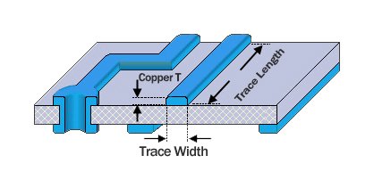
Microstrip Diagram
Formula
Stripline Diagram
Formula
Edge-Coupled Microstrip Diagram
Formula
Edge-Coupled Stripline Diagram
Formula
3. Results
Characteristic Impedance (Zo)-- Ω
Differential Impedance (Zdiff)-- Ω
Disclaimer: These calculations are for estimation purposes only. For final designs, always use professional simulation software.
Usage Guide
- Select Trace Type
Choose from four trace configurations with visual icons:- Microstrip: Single trace on outer layer over a ground plane.
- Stripline: Trace embedded between two ground planes.
- Edge-Coupled Microstrip: Differential pair on outer layer.
- Edge-Coupled Stripline: Differential pair embedded between ground planes.
- Enter Parameters
- Dielectric Constant (εr): Material’s electrical permittivity (e.g., 4.4 for FR-4).
- Trace Thickness (T): Copper thickness in mils (1 oz = 1.37 mils).
- Trace Width (W): Conductor width in mils.
- Substrate Height (H)/Plane Separation (B): Distance to ground plane(s).
- Trace Spacing (S): Appears for differential pairs; distance between traces.
- View Results
- Characteristic Impedance (Zo): For single-ended traces.
- Differential Impedance (Zdiff): For coupled pairs, displayed automatically for edge-coupled types.
Formula Explanations
Single-Ended Microstrip Impedance
Variables:
- Z0: Characteristic impedance of the microstrip line (Ω)
- Key parameter for single-ended signal integrity
- Typical target: 50Ω for RF, 60-70Ω for digital signals
- εr: Substrate dielectric constant
- FR-4: 4.2-4.6 @ 1MHz
- Rogers RO3003: 3.0 @ 10GHz
- H: Substrate height from trace to ground plane (mils)
- Also known as dielectric height
- Thinner H increases Z0 for same trace width
- W: Trace width (mils)
- Wider traces lower Z0 linearly
- Minimum width limited by manufacturing (typically ≥4mils)
- T: Trace thickness (mils)
- 1oz copper: 1.37mils (35μm)
- 2oz copper: 2.74mils (70μm)
Symmetric Stripline Impedance
Variables:
- Z0: Characteristic impedance of stripline (Ω)
- Enclosed between two ground planes for better shielding
- Typical target: 50Ω for controlled impedance designs
- εr: Dielectric constant of core material
- High-frequency materials: εr stability critical
- Example: Isola FR408HR: εr=3.48 @ 10GHz
- B: Total distance between ground planes (mils)
- Also called "plane separation" or "stackup height"
- B = 2H for symmetric stripline with centered trace
- W: Trace width (mils)
- Narrower W increases Z0 in stripline designs
- Width-to-thickness ratio affects field distribution
- T: Trace thickness (mils)
- Thicker traces reduce DC resistance but impact Z0 slightly
- Considered in denominator for geometric correction
Edge-Coupled Microstrip Differential Impedance
Variables:
- Zdiff: Differential impedance of coupled microstrip (Ω)
- Typical targets: 100Ω (USB), 90Ω (Ethernet)
- Depends on both single-ended Z0 and coupling factor
- Z0: Single-ended microstrip impedance (Ω)
- Base impedance of each trace in the pair
- Assumes infinite ground plane for isolation
- S: Spacing between coupled traces (mils)
- Critical for crosstalk and differential impedance control
- S/H ratio determines exponential coupling factor
- Common rule: S ≥ 2W for minimal crosstalk
- H: Substrate height (mils)
- Affects field penetration into substrate
- Lower H increases electromagnetic coupling between traces
Edge-Coupled Stripline Differential Impedance
Variables:
- Zdiff: Differential impedance of coupled stripline (Ω)
- Preferred for high-speed signals requiring low EMI
- Typical value: 100Ω for DDR4 differential pairs
- Z0: Single-ended stripline impedance (Ω)
- Impedance of each trace when isolated
- Calculated using symmetric stripline formula
- S: Spacing between coupled traces (mils)
- Smaller S increases differential impedance due to coupling
- Exponential term: e-1.5S/B models field overlap
- B: Plane separation (mils)
- Total distance between top and bottom ground planes
- B = 2H for centered traces in symmetric stackups
- Larger B reduces coupling effect for same trace spacing
FAQ
What is characteristic impedance (Z0)?
Characteristic impedance is the resistance a signal "sees" as it travels along a transmission line, determined by trace geometry and material properties. A mismatch in Z0 causes signal reflections, degrading integrity. For example, a microstrip with W = 10 mils, H = 6 mils, and εr = 4.4 has:
Z0 =
87
√
(εr + 1.41)
· ln(
5.98 · H
0.8 · W + T
) ≈ 50 Ω
What's the difference between microstrip and stripline?
- Microstrip: Single trace on the surface with a ground plane below.
- Advantages: Easy to route, suitable for low-frequency designs.
- Disadvantages: Radiates EMI, sensitive to board flexing.
- Stripline: Trace sandwiched between two ground planes.
- Advantages: Better EMI shielding, stable at high frequencies.
- Disadvantages: Requires inner layers, more complex to route.
How does trace spacing affect differential impedance?
In edge-coupled pairs, increased spacing S reduces electromagnetic coupling, increasing differential impedance Zdiff. For microstrips:
Zdiff = 2 · Z0 · (1 − 0.347 · e−2.9S/H)
- When S = H: Zdiff ≈ 2Z0 · 0.76
- When S = 3H: Zdiff ≈ 2Z0 · 0.97
What's the difference between single-ended and differential impedance?
| Parameter | Single-Ended (Z0) | Differential (Zdiff) |
|---|---|---|
| Definition | Impedance from trace to ground | Impedance between two coupled traces |
| Typical Values | 50Ω (RF), 60-70Ω (digital) | 100Ω (USB), 90Ω (Ethernet) |
| Application | Single-ended signals (e.g., GPIO) | Differential signals (e.g., LVDS, PCIe) |
| Design Focus | Trace width and ground plane distance | Trace spacing and coupling coefficient |
Differential pairs offer better noise immunity because the differential signal cancels common-mode noise. For example, USB 3.0 requires with and on a 6-mil FR-4 substrate.
Why choose Edge-Coupled Microstrip over Stripline for differential pairs?
- Microstrip: Easier to route, but radiates EMI and is sensitive to board bend.
- Stripline: Better shielding, less crosstalk, and more stable at high frequencies, but requires inner layers.
What role does dielectric constant (εr) play in impedance?
A higher εr increases the effective permittivity of the transmission line, decreasing Z0. For example:
- FR-4 (εr = 4.4): Z0 ≈ 50 Ω for W = 10 mils, H = 6 mils
- Rogers RO3003 (εr = 3.0): Z0 ≈ 58 Ω for the same geometry
Key Dielectric Properties
- εr: Relative permittivity, affects field confinement.
- High-frequency materials: εr stability is critical
- Example: Isola FR408HR: εr = 3.48 @ 10GHz
- Loss Tangent (Df): Energy loss factor, impacts signal attenuation.
- FR-4: Df ≈ 0.02 @ 1MHz
- Rogers RO4350B: Df = 0.004 @ 10GHz
How accurate are these calculations?
Results are based on IPC-standard approximations. Real-world factors like:
- Trace roughness (e.g., 2.1μm RMS)
- Solder mask thickness (0.5-1.0mils)
- Manufacturing tolerances (±10% for trace width)
- Dielectric thickness variation (±5%)