Pregúntele a un ingeniero «qué es SMT» y generalmente escucha «tecnología de montaje en superficie». Eso es correcto. Pero si te detienes en el acrónimo, te estás perdiendo algo SMT en realidad significa Diseñado, construido, probado y pagado como una tabla. Este artículo explica la Definición de SMT En términos que son importantes para todos los que diseñan, ordenan o eliminan las placas de circuito impreso ensamblados.
La definición simple de SMT
smt (Tecnología de montaje en superficie) es un método de montaje de PCB en el que los componentes se montan directamente en la superficie de una placa de circuito impreso sin que pasen los tubos por los orificios. Esto reemplazó a la tecnología continua (THT) como el método de producción dominante de la década de 1980 y ahora representa la gran mayoría del ensamblaje de placas de circuito comercial.
La diferencia clave: conjunto de orificios pasantes, las líneas de componentes se apagan mediante taladre agujeros y soldados en el lado opuesto. Componentes sentarse en SMT encima Impreso con almohadillas con soldadura en pasta y soldado durante el reflujo. Sin agujeros, sin poda y una densidad de componentes dramáticamente mayor.
¿Qué cambios «SMT» en el diseño de PCB
Si creciste con la creación de prototipos de orificio pasante, cambiar a SMT significa repensar los múltiples hábitos de diseño:
- El enrutamiento de seguimiento se vuelve más estrecho. Las almohadillas SMD son más pequeñas y cercanas. Puede colocar un condensador de desacoplamiento dentro de un milímetro de un pin de alimentación IC, lo que mejora la integridad de la señal en formas que rara vez se logran los diseños.
- Ambos lados se vuelven utilizables. Los componentes de SMT pueden llenar tanto la parte superior como la inferior de una placa. Esto duplica el área efectiva sin aumentar el esquema de PCB, lo que importa mucho en productos de consumo compactos.
- Las vías se convierten en herramientas de enrutamiento, no en anclajes de componentes. Dado que los componentes no necesitan orificios pasantes plateados, los vias se liberan únicamente para transiciones de capa y gestión térmica.
- Cambios de diseño térmico. Los componentes SMD disipan el calor en los planos de cobre a través de sus almohadillas en lugar de cables de plomo. Un vertido de cobre adecuado debajo de una parte de potencia SMD hace más para enfriar que un clip de disipador de calor de orificio pasante.
Si ya ha publicado un diseño orientado a SMT y desea moverlo a la producción sin rediseñar toda la lista de materiales, Servicio de montaje de PCBS inverso Contiene tableros de tecnología mixta donde existen SMT y los componentes de tránsito uno al lado del otro.
SMT vs. agujero pasante: la realidad del piso de montaje
Los Definición de SMT En la línea de montaje es lo más importante. Lo siguiente cambia cuando un diseño de orificio pasante cambia a SMT:
| Aspecto | a través del hoyo | petardazo |
|---|---|---|
| Colocación de componentes | Dispositivos de soldadura manual o de onda | Pick-and-Place automatizado con miles de CPH |
| Soldadura | Soldadura de eje o manual | Horno de reflujo con perfil de calor controlado |
| Catering inmobiliario | Consume ambos lados con agujeros de plomo | Los componentes se sientan en la superficie, se pueden usar en ambos lados |
| Tamaño de componente mínimo | ~ 0805 equivalente | hasta 01005 (0,4 x 0,2 mm) |
| Rework difficulty | Simplemente con un soldador | Requiere aire caliente, precalentamiento o estación de reelaboración dedicada |
| fuerza mecánica | Más fuerte (Conducir a través del agujero) | Más débil contra cizallamiento, se basa en la adhesión de la almohadilla |
En la mayoría de las producciones de más de unas pocas docenas de unidades, SMT gana a velocidad, consistencia y costo por unidad. El compromiso existe de antemano: la plantilla, la programación de pick-and-place y el perfil de reflujo se llevan a cabo frente a los primeros barcos de la junta.
Componentes SMD: lo que se ensambla
Los componentes utilizados en Tecnología de montaje en superficie se llaman SMDS – dispositivos montados en superficie. Los tipos de paquetes SMD comunes son:
- Chips pasivos (resistencias, condensadores, inductores): estándares como 0402, 0603, 0805. El número es la huella en centésimas de pulgada — un 0603 mide 0.06″ x 0.03″.
- SOIC, SSOP, Tssop: IC de ala de gaviota, los caballos de batalla de circuitos analógicos y de señal mixta.
- QFP, LQFP, TQFP: ICS cuadrados con cables en cuatro lados, común en microcontroladores de hasta ~200 pines.
- QFN, DFN: paquetes sin plomo con almohadillas térmicas expuestas debajo. Más difícil de soldar a mano, excelente rendimiento térmico.
- BGA: Las matrices de rejilla de bolas ocultan las bolas de soldadura debajo del paquete. Imposible inspeccionar visualmente después del reflujo sin rayos X.
- 0201, 01005: Pasivos ultra miniatura utilizados en teléfonos y wearables. La soldadura manual no es realista.
Elegir el paquete adecuado es igualmente una decisión eléctrica. Si el fabricante de su contrato no puede colocar las piezas 0201 de manera confiable, no las especifique.
El proceso de montaje de SMT en cuatro pasos
entender el Tecnología de montaje en superficie El flujo de trabajo le ayuda a escribir mejores reglas de DFM:
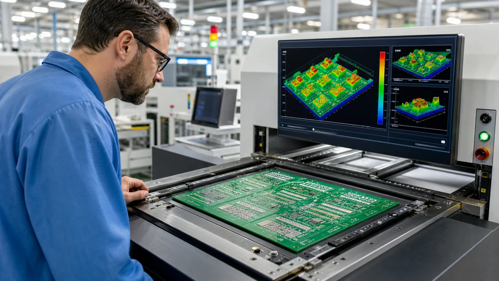
- Impresión en pasta de soldadura. Una plantilla de acero inoxidable se alinea sobre la PCB desnuda. La pasta de soldadura se exprime a través de ella, depositando pasta solo en almohadillas de componentes. El grosor de la plantilla, el diseño de apertura y la reología de la pasta controlan el volumen de depósito.
- pick-y-place. Una máquina de alta velocidad recoge los SMD de los carretes o bandejas de cinta utilizando boquillas de vacío y los coloca sobre las almohadillas pegadas. La precisión de colocación suele ser superior a 50 µm para las máquinas modernas.
- Soldadura por reflujo. La placa poblada viaja a través de un horno de reflujo con zonas de calefacción controladas. El perfil térmico aumenta, se absorbe para activar el flujo, se eleva por encima de Liquidus (~217 °C para la soldadura sin plomo SAC305) y luego se enfría a una velocidad controlada. La pasta se funde, humedece las almohadillas y las terminaciones de los componentes y se solidifica en juntas de soldadura fiables.
- inspección. Comprobaciones de inspección óptica automatizada (AOI) para puentes de soldadura, lápidas, humectación insuficiente y compensaciones de componentes. Las tablas con BGA o juntas ocultas también pueden pasar por la inspección de rayos X.
Cuando diseñe su primera placa SMT y busque un socio de fabricación que asuma problemas de DFM antes de crear prototipos, ReversePcbs Verificación DFM Problemas de plantilla, bloques y colocación de banderas antes de tiempo.
Defectos comunes de SMT y lo que te dicen
Cada defecto SMT tiene una causa raíz. Aprender a leer te hace más rápido para solucionar problemas de producción:
- Tombstoning: un extremo de un componente de chip se levanta de la almohadilla durante el reflujo. Usually caused by uneven heating (one pad reaches liquidus first) or pad geometry imbalance. Solución: Ecualizar tamaños de almohadillas y alivio térmico en ambos lados.
- Puente de soldadura: El exceso de soldadura conecta las almohadillas adyacentes. Causas comunes: demasiada pasta, apertura de plantilla demasiado ancha o espaciado insuficiente entre las almohadillas.
- Humectación insuficiente: la soldadura no formó un filete adecuado. Revise la oxidación de la almohadilla, la edad de la pasta o el perfil de reflujo: si la placa nunca llegó a Liquidus el tiempo suficiente, falla la humectación.
- Cabeza en almohada: las bolas BGA y la pasta se derriten por separado sin fusionarse. Por lo general, un problema de perfil de reflujo donde el paquete se deforma y las bolas pierden contacto con la pasta durante la fase líquida.
- Vaciado: Burbujas de gas atrapadas en la junta de soldadura debajo de BGA o QFN. El exceso de flujo, la humedad o una tasa de rampa agresiva pueden causar vacíos.
Reglas de diseño que previenen los dolores de cabeza SMT
Si sigue estas reglas, su rendimiento de SMT será mediblemente mayor:
- Espaciado de pad-to-pad: mantenga al menos 0,2 mm entre las almohadillas adyacentes, a menos que su FAB y su ensamblador aprueben un espacio más estricto.
- Liquidación de componente a borde: piezas dentro de los 3 mm de la placa de riesgo de las tumbas de calentamiento desigual cerca del riel. Muévalos hacia adentro o agregue alivio térmico.
- Marcas fiduciales: coloque tres fiduciales globales (uno en cada esquina, asimétricamente) más fiduciales locales cerca de piezas de tono fino. Las máquinas pick-and-place las utilizan para la alineación óptica.
- Reducción de la abertura de la plantilla: para QFPS de tono fino y piezas de paso de 0,5 mm, reduzca el ancho de apertura en un 10 a 20% para evitar el puente. El ingeniero de plantillas de su ensamblador debería confirmar esto.
- Alivio térmico en grandes áreas de cobre: una almohadilla conectada directamente a un gran plano de tierra absorberá el calor durante el reflujo, causando juntas frías. Utilice radios de alivio térmico.
Para obtener más información sobre la disciplina «Diseño para la fabricación», consulte ReversePCBS Guía DFMuna
Si SMT no es la respuesta correcta
SMT domina el montaje de PCB, pero no es universal. A través de las victorias de hoyos en estos escenarios:
- Conectores y puntos de tensión mecánica. Los puertos USB, los conectores de barril y los bloques de terminales experimentan una fuerza de inserción repetida. El montaje de orificio pasante proporciona un anclaje mecánico que las almohadillas SMT no pueden igualar.
- Componentes de alta potencia. Los grandes transformadores, los transistores de potencia sin disipación térmica y las bobinas de relé suelen utilizar orificios pasantes tanto para la capacidad de corriente como para la gestión térmica.
- Creación de prototipos y construcciones únicas. Se puede factible la soldadura manual 0603 pasivas bajo un microscopio. Soldar a mano Un QFN de 64 pines no lo es. La creación de prototipos de orificio pasante sigue siendo más rápida para el trabajo de bajo volumen.
- Diseños heredados de tecnología mixta. Muchas placas industriales y automotrices combinan secciones lógicas SMT con potencia de orificio pasante y secciones de E/S. Estos son totalmente fabricables con las líneas de tecnología mixta de hoy.
Preguntas frecuentes
¿Qué significa SMT?
SMT significa tecnología de montaje en superficie. Es el método de ensamblaje de PCB donde los componentes se montan directamente sobre la superficie del tablero en lugar de los orificios perforados.
¿Cuál es la diferencia entre SMT y SMD?
SMT se refiere al montaje tecnología (el proceso). SMD se refiere a la dispositivo (el componente en sí). Un SMD, o dispositivo de montaje en superficie, es cualquier componente diseñado para el ensamblaje de SMT.
¿Por qué SMT reemplazó el orificio pasante para la mayoría de los ensamblajes de PCB?
SMT permite una mayor densidad de componentes, ensamblaje automatizado de alta velocidad, tamaños de placa más pequeños y menor costo por unidad. También permite componentes en ambos lados de la placa, que no pueden igualar.
¿Puedes mezclar SMT y pasante en la misma placa?
Sí. Los tableros de tecnología mixta son comunes en electrónica industrial y automotriz. El lado SMT se refluye primero, luego se colocan componentes de orificio pasante y se sueldan ondulados o se soldan a mano.
¿Cuál es el tamaño de componente SMD más pequeño?
01005 (0,4 x 0,2 mm) es el tamaño pasivo más pequeño ampliamente disponible. Estos requieren equipos especializados de pick-and-place y se utilizan principalmente en teléfonos inteligentes, dispositivos portátiles y dispositivos médicos implantables.
¿Cuál es la definición de SMT en la fabricación de electrónica?
En la fabricación de electrónica, la definición de SMT es un proceso de ensamblaje en el que se imprime la pasta de soldadura en las almohadillas de PCB, los componentes se colocan en la pasta mediante equipos automatizados y todo el conjunto pasa a través de un horno de reflujo para formar juntas de soldadura permanentes sin cables de orificio pasante.