Otomatisasi Desain Elektronik (EDA) adalah kategori yang digunakan insinyur perangkat lunak untuk merancang, mensimulasikan, dan memverifikasi sistem elektronik sebelum satu PCB dibuat. Jika menurut Anda EDA hanya berarti “pengambilan skematis”, Anda kehilangan sebagian besar dari apa yang sebenarnya dilakukan oleh toolchain EDA modern. Artikel ini menjelaskan apa yang dilakukan alat otomasi desain elektronik, bagaimana mereka berbeda satu sama lain, dan apa yang harus dicari saat memilih platform EDA untuk pekerjaan PCB.
Apa yang Sebenarnya Dicakup Otomatisasi Desain Elektronik
Minimal, an Otomatisasi Desain Elektronik Toolchain menangani empat tahap:
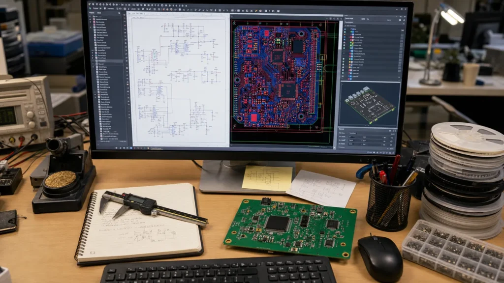
Pengambilan skema: Menggambar sirkuit logis. Di sinilah Anda menempatkan simbol, koneksi kabel, dan menetapkan nilai komponen. Alat skematis yang baik juga mengelola lembar hierarkis, pemeriksaan aturan desain (DRC), dan pemeriksaan aturan kelistrikan (ERC).
Tata letak PCB: Menerjemahkan skema ke dalam papan fisik. Editor PCB menempatkan jejak kaki, rute jejak tembaga, mendefinisikan lapisan bidang, dan menerapkan aturan desain untuk izin, impedansi, dan kemampuan manufaktur.
Simulasi dan analisis: Simulasi SPICE untuk sirkuit analog, analisis integritas sinyal untuk analisis digital berkecepatan tinggi, simulasi termal, dan jaringan distribusi daya (PDN). Ini berjalan di dalam atau di samping alat EDA.
Output manufaktur: Menghasilkan file Gerber, file bor, data pick-and-place, dan gambar perakitan. Kesalahan pada tahap ini membuat penolakan fabrikasi.
Untuk lebih lanjut tentang praktik terbaik skematik, lihat Panduan Desain Skema PCB ReversePCBS.
Platform EDA Utama untuk Desain PCB
Lanskap EDA terbagi secara kasar menjadi tiga tingkatan, dan memilih yang salah untuk proyek Anda menyebabkan rasa sakit yang nyata:
| Tingkat | Alat | terbaik untuk | Keterbatasan |
|---|---|---|---|
| Sumber terbuka / gratis | kicad, easyeda, librepcb | Proyek hobi, perangkat keras terbuka, 2-6 papan lapisan | Simulasi lanjutan terbatas, manajemen perpustakaan yang kurang kuat |
| Profesional kelas menengah | Altium Designer, Orcad, Pads | Papan lapisan 4-16 profesional, desain kecepatan tinggi, alur kerja tim | Biaya berlangganan, kurva belajar yang curam |
| Perusahaan / RF-Spesialisasi | Cadence Allegro, Mentor Xpedition, Iklan | Multilayer kompleks, RF / microwave, HDI, kaku-flex | Biaya sangat tinggi, membutuhkan staf pendukung CAD khusus |
KICAD telah menutup celah dengan alat kelas menengah untuk banyak desain. Sekarang menjadi pilihan profesional yang layak untuk papan hingga sekitar 8 lapisan, asalkan tim Anda merasa nyaman dengan alur kerja perpustakaannya. Jika Anda merancang papan digital berkecepatan tinggi dengan memori DDR atau pasangan diferensial pada beberapa GHz, alat integritas sinyal altium atau tingkat irama menjadi lebih sulit untuk diganti.
Alur kerja skema-ke-PCB dalam praktik
Inilah tampilan alur kerja EDA untuk proyek PCB biasa:
membuat skema. Tempatkan simbol, jaring kawat, tetapkan jejak kaki, dan jalankan ERC untuk menangkap pin yang tidak terhubung atau output yang bertentangan.
menghasilkan netlist. Netlist adalah daftar yang dapat dibaca mesin dari setiap komponen dan koneksi. Alat tata letak PCB mengimpornya.
komponen tempat. Posisikan jejak kaki pada garis besar papan. Kelompokkan bagian terkait, arahkan konektor dengan benar, dan sisakan ruang untuk lubang pemasangan dan zona penyimpanan.
jejak rute. Hubungkan bantalan sesuai dengan netlist, menghormati aturan izin, persyaratan lebar jejak, dan target impedansi. Alat EDA modern termasuk perutean otomatis, tetapi jaring kritis harus selalu dirutekan dengan tangan.
Jalankan DRC. Pemeriksa aturan desain memverifikasi bahwa tidak ada jejak yang melanggar izin, tidak ada pad yang kehilangan koneksi, dan setiap jaringan dialihkan sepenuhnya. Melewati DRC adalah persyaratan minimum sebelum mengirim papan ke fabrikasi.
menghasilkan file manufaktur. Ekspor gerbers, file bor NC, BOM, dan gambar perakitan. Periksa kembali penampil Gerber — kesalahan pada tahap ini mahal.
Jika Anda berpindah dari skema ke PCB di altium secara khusus, Panduan langkah demi langkah ini berjalan melalui proses penuh.
Apa yang Harus Diperhatikan Saat Memilih Alat EDA
Fokus pada apa yang sebenarnya memengaruhi proyek Anda, bukan pemasaran jumlah fitur:
Kualitas dan Manajemen Perpustakaan: Apakah alat ini dilengkapi dengan jejak terverifikasi untuk komponen yang benar-benar Anda gunakan, atau akankah Anda menghabiskan waktu berjam-jam untuk membuat simbol dari lembar data? Perpustakaan yang lemah membuang lebih banyak waktu daripada fitur simulasi yang hilang.
Kemampuan Aturan Desain: Dapatkah Anda menentukan aturan berdasarkan kelas bersih, pasangan diferensial, dan wilayah? Jika Anda membutuhkan impedansi terkontrol, apakah alat menghitung geometri jejak dari tumpukan Anda?
Kolaborasi: Bisakah beberapa insinyur bekerja pada proyek yang sama? apakah itu mendukung kontrol versi? Integrasi GIT semakin standar dalam alat EDA modern.
Keandalan keluaran manufaktur: Apakah ekspor Gerber cocok dengan papan yang dirancang? Beberapa alat secara diam-diam menerapkan koreksi aturan desain selama output yang mengubah papan. Verifikasi di Gerber Viewer setiap saat.
Integrasi Simulasi: Jika Anda mengandalkan simulasi SPICE, apakah alat tersebut mengintegrasikannya secara asli, atau Anda perlu mengekspor netlist ke simulator eksternal?
Kesalahan umum EDA yang mencapai fabrikasi
Jaring yang tidak dialihkan melewati DRC: Beberapa alat memungkinkan jaring yang tidak dialihkan untuk melewati DRC jika ditandai sebagai “tidak ada koneksi.” Verifikasi setiap jaringan secara visual atau dengan laporan konektivitas.
Footprint Pin 1 Ketidakcocokan: Simbol skema dan jejak PCB tidak setuju pada orientasi PIN 1. Ini adalah penyebab paling umum dari kegagalan papan revisi pertama. Selalu verifikasi indikator PIN 1 secara visual pada setiap jejak IC.
Bantalan tumpang tindih silkscreen: silkscreen yang dicetak pada bantalan tembaga mencegah penyolderan. Sebagian besar alat memiliki aturan izin silkscreen-to-pad — aktifkan.
Impedansi tak tertandingi: Geometri jejak dalam tata letak tidak menghasilkan impedansi target karena tumpukan didefinisikan secara tidak benar di alat. Verifikasi impedansi dengan tumpukan aktual fabrikator, bukan default alat.
Pertanyaan yang sering diajukan
Apa itu Otomatisasi Desain Elektronik?
Electronic Design Automation (EDA) adalah kategori perangkat lunak yang digunakan untuk merancang sistem elektronik, termasuk penangkapan skematik, tata letak PCB, simulasi sirkuit, dan pembuatan file manufaktur. Alat EDA sangat penting untuk pengembangan PCB modern.
Apakah KiCad Cukup Baik untuk Desain PCB Profesional?
Ya, KICAD sekarang mampu mendesain PCB kelas profesional untuk papan hingga sekitar 8 lapisan. Ini mendukung perutean pasangan diferensial, penyetelan panjang, dan visualisasi 3D. Untuk desain kecepatan sangat tinggi yang memerlukan simulasi integritas sinyal tingkat lanjut, alat altium atau irama memberikan analisis yang lebih dalam.
Apa perbedaan antara Schematic Capture dan PCB Layout?
Skema Capture adalah fase desain logis di mana Anda menentukan koneksi komponen dan fungsi sirkuit. Tata letak PCB adalah fase desain fisik di mana Anda menempatkan komponen, merutekan jejak tembaga, dan menyiapkan papan untuk manufaktur.
Apakah saya memerlukan simulasi di alat EDA saya?
Untuk papan digital sederhana, simulasi adalah opsional. Untuk sirkuit analog, catu daya, atau desain digital berkecepatan tinggi, simulasi SPICE dan analisis integritas sinyal menangkap masalah sebelum fabrikasi dan menghemat putaran revisi.
File apa yang dihasilkan alat EDA untuk manufaktur?
Output manufaktur standar termasuk file Gerber (format RS-274X atau X2) untuk setiap lapisan tembaga, masker solder, dan silkscreen; NC file bor; file pick-and-place (centroid) untuk perakitan otomatis; dan tagihan bahan (BOM).