Overview of Leadless Chip Carrier (LCC)
Explore LCC technology—a key driver for the miniaturization and performance enhancement of modern electronic devices. This guide will walk you through its unique design, superior performance, and widespread applications.
⚡️ Superior Electrical Performance
Short signal paths for lower latency and interference, ideal for high-speed circuits.
📏 Compact Footprint
The leadless design saves significant PCB space, enabling higher component density.
🌡️ Efficient Thermal Management
Direct contact with the PCB ensures rapid heat dissipation for stable operation.
What is a Leadless Chip Carrier?
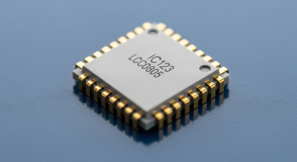
A Leadless Chip Carrier (LCC) is an integrated circuit (IC) package that, as its name suggests, lacks traditional external leads. Instead, it utilizes contact pads or metallized half-holes on its sides or bottom for direct soldering onto a printed circuit board (PCB).
Metallized Half-Holes
This feature involves vertical channels with a plated surface that extend from the top to the bottom of the package side. These half-holes act as robust solder points, allowing for precise surface-mount soldering and providing a large, reliable contact area for electrical signals.
Contact Pads
LCCs are equipped with flat, metallized contact pads, typically located on the bottom or perimeter of the package. These pads serve as the direct electrical and thermal interface with the PCB, minimizing signal path length and enabling efficient heat transfer.
Material-Based Performance
The choice of material significantly impacts the performance of an LCC. While Plastic LCC (PLCC) is a common alternative, Ceramic LCC (CLCC) offers unique advantages for demanding applications.
Ceramic LCC (CLCC)
 1")
5962-1721401VXC | Photo by TI
- Hermetic Sealing: Provides an airtight, moisture-resistant package, essential for high-reliability military and aerospace applications.
- Superior Thermal Management: Ceramic materials have excellent thermal conductivity, efficiently drawing heat away from the die.
- Mechanical Robustness: The rigid ceramic body offers high resistance to physical stress and environmental changes.
- Higher Cost: Due to the complexity and material properties, CLCCs are significantly more expensive.
Plastic LCC (PLCC)
 2")
TL16C452FNR | Photo by TI
- Cost-Effectiveness: Made from molded plastic compounds, making them a more economical choice for consumer electronics.
- Familiar Manufacturing: Utilizes well-established plastic molding processes, leading to high-volume production at lower cost.
- Non-Hermetic: Unlike ceramic, plastic does not provide a hermetic seal, making it susceptible to moisture ingress.
- Less Robust: The plastic body is more vulnerable to mechanical stress and thermal mismatch with the PCB.
LCC's Core Value Proposition
The technical superiority of LCC is the fundamental reason for its widespread adoption. Click on the cards below to delve into its key advantages in electrical performance, thermal dissipation, and miniaturization.
Electrical Performance
By eliminating external leads, LCC significantly reduces parasitic inductance and resistance. This ensures the integrity of high-speed signals.
Thermal Management
Its pads are soldered directly to the PCB, creating a broad and highly efficient thermal path to ensure stable device operation.
Miniaturization & Density
In space-constrained devices, the compact size of the LCC is a huge advantage, enabling more functions in a limited PCB area.
Interactive Technical Comparison
LCC does not exist in a vacuum; understanding its position among various packaging technologies is crucial. With the interactive chart below, you can visually compare LCC with PLCC, BGA, and QFP on key performance metrics. Click the buttons below to switch between different comparison dimensions.
Key Application Areas
With its unique technical advantages, LCC plays an indispensable role in many frontier technology fields. This section showcases specific use cases for LCC across different industries. Click the cards below to learn more details.
📡 5G Communication
In the RF modules of 5G base stations, LCC's high-frequency performance ensures low-loss, low-distortion transmission of massive data streams.
💻 High-Performance Computing
In servers and supercomputers, LCC-packaged memory and processor chips enable high-speed data access and high-density integration.
🚗 Automotive Electronics
In self-driving sensors and in-vehicle infotainment systems, LCC provides the high reliability required in harsh environments.
💡 Internet of Things (IoT)
The small size and high integration of LCC make it an ideal choice for space-constrained IoT sensors and edge devices.
🛰️ Aerospace & Defense
Ceramic LCC packages, due to their superior reliability and hermeticity, are widely used in military and aerospace applications.
🤖 Edge Computing & AI
In devices requiring local, real-time AI processing, LCC provides the necessary high-speed data processing capabilities.
Manufacturing & Design Considerations
Successfully integrating an LCC into a product requires a deep understanding of its manufacturing process, potential challenges, and reliability measures. Click on each step below to get a detailed breakdown of the process.
Detailed Manufacturing Process
Key Challenges & Solutions
LCC manufacturing demands extremely high precision, and high-performance materials like ceramic come at a significant cost. Additionally, in applications like automotive or aerospace, stress from thermal expansion coefficient (CTE) mismatch between the package and the PCB is a primary risk for solder joint failure.
To counter these challenges, several strategies are employed to enhance reliability and manufacturability.
💡 Solutions for Reliability
- LCC Sockets: Provide a removable interface, avoiding direct soldering and simplifying prototyping and field maintenance.
- Advanced Thermal Management: Utilizes thermal vias, heat sinks, and thermal interface materials (TIMs) to ensure efficient heat transfer and prevent overheating.
- Mechanical Reinforcement: Techniques like underfilling or glob-topping can be applied to reinforce solder joints, improving their resistance to mechanical stress and thermal cycling.
- Vibration Isolation: For applications with high-vibration, such as automotive or military, specialized PCB layouts and mechanical mounts are used to protect the package from stress.