Sebuah Perangkat pemasangan permukaan Bukan hanya bagian elektronik yang kebetulan muat di papan tulis. itu adalah keputusan manufaktur. Gaya paket memengaruhi pelepasan stensil, toleransi penempatan, akses inspeksi, kesulitan pengerjaan ulang, perilaku termal, dan bahkan apakah pembuatan pilot mengajarkan Anda sesuatu yang berguna.
Itu sebabnya memilih paket SMD berdasarkan ukuran tapak saja sudah cukup jarang. Insinyur sering mengoptimalkan area papan atau biaya unit dan menemukan kemudian bahwa penalti yang sebenarnya muncul dalam pengaturan pengumpan, sambungan tersembunyi, atau waktu perbaikan. Panduan ini berfokus pada cara memilih paket pemasangan permukaan yang dapat didukung oleh proses perakitan Anda dengan andal.
Apa yang Sebenarnya Diubah oleh Perangkat Pemasangan Permukaan
Definisi dasarnya langsung: SMD adalah komponen yang dirancang untuk pemasangan langsung ke bantalan permukaan daripada lubang melalui berlapis. Tetapi pertanyaan rekayasa yang penting adalah apa yang diubah oleh pilihan untuk membangun.
Kepadatan papan meningkat. Bagian yang lebih kecil dan populasi sisi ganda membuat desain yang ringkas menjadi praktis.
Otomatisasi menjadi default. Setelah pitch paket cukup baik, asumsi penempatan dan reflow mulai mendorong desain.
perubahan inspeksi. Lead sayap camar mudah diperiksa secara visual. Bantalan termal tanpa timah dan BGA tidak.
Pengerjaan ulang menjadi tergantung pada paket. Resistor 0603 dan QFN berpitch halus keduanya SMD, tetapi keduanya tidak menuntut alat perbaikan atau keterampilan operator yang sama.
ReversePCBS Ikhtisar SMT menjelaskan proses itu sendiri. Masalah pemilihan paket lebih sempit: Gaya perangkat mana yang memberi Anda hasil listrik yang Anda inginkan tanpa membuat perakitan lebih sulit dari yang seharusnya?
Bentuk timah lebih penting daripada yang diakui banyak BOM
Pilihan paket sering dimulai dengan sistem prospek, karena sistem prospek mengontrol visibilitas pembasahan, perilaku self-alignment selama reflow, dan akses pengerjaan ulang.
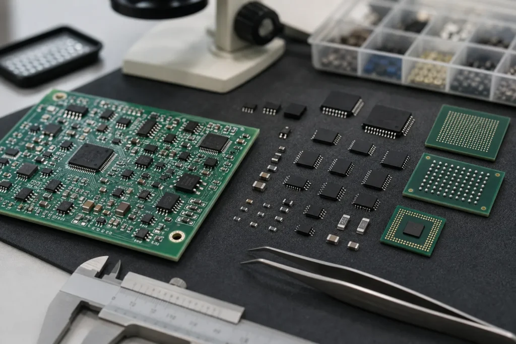
Paket SOIC, TSSOP, dan QFP memiliki prospek yang terlihat. Mereka memaafkan dalam pemeriksaan dan lebih mudah untuk menyelidiki atau menyentuh daripada paket tanpa timah.
Paket QFN dan DFN menghemat ruang dan sering meningkatkan kinerja termal, tetapi bantalannya bersembunyi di bawah bodi. Itu meningkatkan taruhannya untuk disiplin pola daratan, strategi tempel, dan kontrol pengosongan pad termal.
Paket BGA memaksimalkan jumlah PIN dan kepadatan perutean, tetapi mereka menukar inspeksi visual langsung. Jika produk tidak dapat membenarkan akses sinar-X atau perencanaan pengerjaan ulang yang cermat, BGA mungkin merupakan kenyamanan yang salah.
Pasif chip tampak sederhana sampai ukurannya menjadi terlalu agresif. Perpindahan dari 0603 ke 0201 dapat mengubah stabilitas penempatan, pelepasan stensil, dan kepraktisan layanan lapangan lebih dari itu mengubah desain listrik.
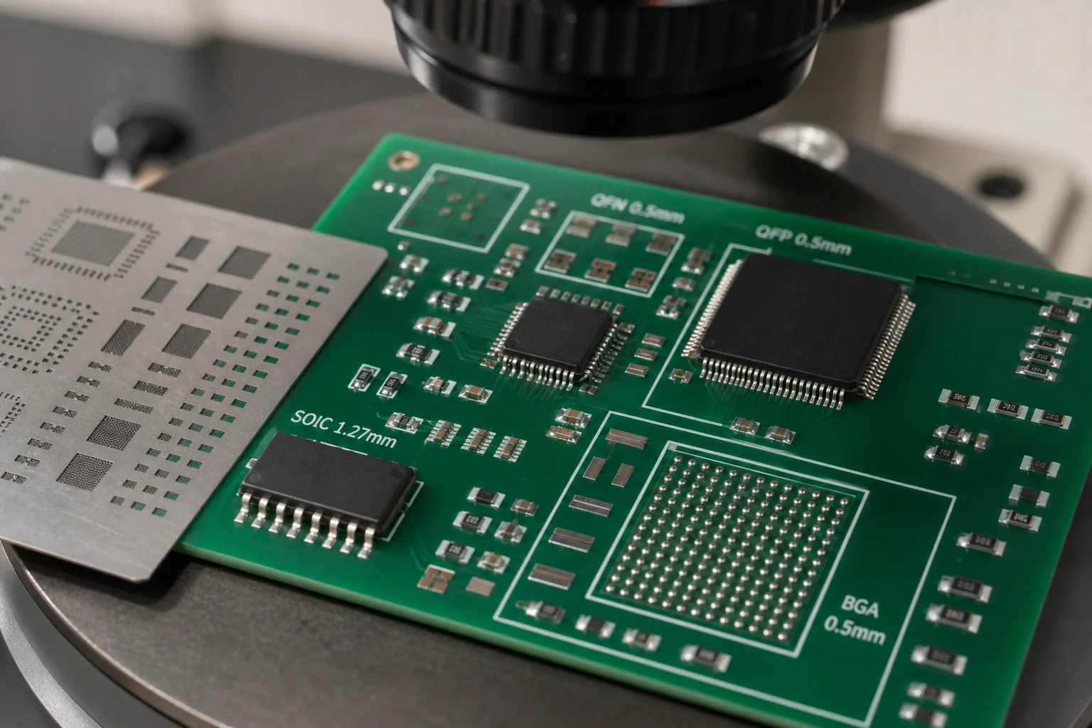
Gunakan urutan pilihan ini alih-alih memilih berdasarkan ukuran terlebih dahulu
Keputusan paket praktis biasanya bekerja lebih baik dalam urutan ini:
Mulai dengan fungsi dan beban termal. Perangkat daya dan IC yang peka terhadap panas mungkin memerlukan bantalan terbuka atau antarmuka tembaga yang lebih besar.
Periksa penempatan dan kemampuan inspeksi. Jika lingkungan build tidak mendukung pitch yang sangat halus, pasif ultra-kecil, atau validasi x-ray, jangan memilih paket tersebut dengan santai.
Pertimbangkan pengerjaan ulang dan layanan. Paket yang sedikit lebih besar dapat menghemat waktu utama dalam debug prototipe, perbaikan lapangan, dan kontrol perubahan rekayasa.
Hanya kemudian mengoptimalkan area dan biaya. Area papan penting, tetapi tidak cukup untuk membenarkan paket yang mempersempit jendela proses tanpa manfaat tingkat produk.
Kesalahan paket SMD umum yang merusak hasil
Menentukan bagian tanpa timah tanpa memberikan perhatian yang cukup pada thermal pad. Pad yang terbuka adalah bagian dari tantangan perakitan, bukan renungan.
Menggunakan pasif terkecil yang tersedia untuk alasan kosmetik. Paket kecil mengesankan tangkapan layar tata letak lebih dari mereka meningkatkan banyak produk nyata.
mengabaikan akses inspeksi. Jika sambungan kritis tidak dapat dilihat atau diuji, prosesnya harus mengimbangi di tempat lain.
Mencampur permintaan paket yang sangat berbeda pada satu papan tanpa perencanaan proses. Papan yang menggabungkan siput termal besar, lead pitch ultra-halus, dan 0201 pasif membutuhkan stensil dan strategi profil yang disengaja.
Untuk tim yang masih perlu memutuskan apakah bagian through-hole adalah jawaban mekanis yang lebih baik, Pengorbanan melalui lubang versus permukaan-mount Tetap layak ditinjau sebelum melakukan BOM.
Pilih paket yang dapat dibangun, diperiksa, dan diperbaiki oleh pabrik.
Terbaik Perangkat pemasangan permukaan Pilihan jarang merupakan paket terkecil, terbaru, atau paling ringkas. Ini adalah paket yang sesuai dengan kebutuhan listrik sambil tetap berada di dalam jendela manufaktur yang masuk akal. Ketika para insinyur membuat keputusan paket dengan mempertimbangkan perakitan, inspeksi, dan perbaikan, dewan menjadi lebih mudah untuk diluncurkan dan lebih mudah dipercaya dalam produksi.
Apa itu perangkat pemasangan permukaan?
Perangkat pemasangan permukaan, atau SMD, adalah komponen yang dirancang untuk disolder langsung ke bantalan PCB tanpa kabel yang melewati lubang yang dibor.
Apa perbedaan antara SMT dan SMD?
SMT adalah metode perakitan, sedangkan SMD adalah komponen yang dibangun untuk metode itu. Anda memilih paket SMD, kemudian memproduksinya dengan proses SMT.
Mengapa pilihan paket memengaruhi kemampuan manufaktur?
Gaya paket mempengaruhi desain stensil, akurasi penempatan, akses inspeksi, kinerja termal, dan kesulitan pengerjaan ulang. Dua bagian yang setara secara elektrik dapat menciptakan risiko perakitan yang sangat berbeda.
Apakah paket tanpa timah selalu lebih baik daripada paket bertimbal?
Tidak. Paket tanpa timah dapat menghemat ruang dan meningkatkan perilaku termal, tetapi juga mengurangi akses inspeksi visual dan sering kali membuat pengerjaan ulang lebih keras. Pilihan terbaik tergantung pada produk dan lingkungan bangunan.
Kapan seorang insinyur harus menghindari ukuran pasif terkecil yang tersedia?
Hindari pasif ultra-kecil ketika papan tidak membutuhkannya atau ketika kemampuan penempatan, akses pengerjaan ulang, atau keandalan layanan lapangan akan meningkat dengan paket yang sedikit lebih besar seperti 0603, bukan 0201.