pek iyi Yüzeye montaj cihazı Tahtaya sığan sadece elektronik kısım değil. Bu bir üretim kararıdır. Paket stili, şablonların serbest bırakılmasını, yerleştirme toleransını, inceleme erişimini, yeniden işleme zorluklarını, termal davranışı ve pilotluğun size yararlı bir şey öğretip öğretmediğini bile etkiler.
Bu nedenle sitenin boyutuna göre SMD paketini seçmek oldukça nadirdir. Mühendisler genellikle pano alanını veya birim maliyetini optimize eder ve daha sonra gerçek cezaların besleyici ayarlarında, gizli bağlantılarda veya onarım zamanlarında göründüğünü bulur. Bu kılavuz, montaj işleminizin güvenilir bir şekilde destekleyebileceği bir yüzey montaj paketini nasıl seçeceğinize odaklanır.
Yüzeye montaj cihazının gerçekte neyi değiştirdiği
Temel tanım doğrudandır: SMD, katmanlı deliklerden ziyade yüzey yatağına doğrudan montaj için tasarlanmış bir bileşendir. Ancak önemli bir mühendislik sorusu, inşa edilecek seçimin ne olduğudur.
tahta yoğunluğu artar. Daha küçük parçalar ve çift taraflı popülasyonlar, kompakt tasarımları pratik hale getirir.
Otomasyon varsayılandır. Paket adımı yeterince iyi olduktan sonra, yerleştirme ve yeniden akış varsayımı tasarımı zorlamaya başlar.
Muayene değişikliği. Martı kanadı uçlarının görsel olarak incelenmesi kolaydır. Kurşunsuz termal pedler ve BGA no.
Yeniden işleme pakete bağımlı hale gelir. Dirençler 0603 ve QFN, her iki SMD’ye de iyi bir şekilde yerleştirilmiştir, ancak her ikisi de aynı onarım araçlarını veya operatör becerilerini talep etmez.
Ters PCB’ler Genel Bakış SMT Sürecin kendisini açıklayın. Paketi seçme sorunu daha dardır: Hangi tip cihaz, montajı olması gerekenden daha zor hale getirmeden size istediğiniz elektrik sonuçlarını verir?
Kalay şekli birçok bombanın kabul ettiğinden daha önemlidir
Paket seçenekleri genellikle potansiyel sistemle başlar, çünkü potansiyel sistem ıslanma görünürlüğünü, yeniden akış sırasında kendi kendine hizalama davranışını ve yeniden işleme erişimini kontrol eder.
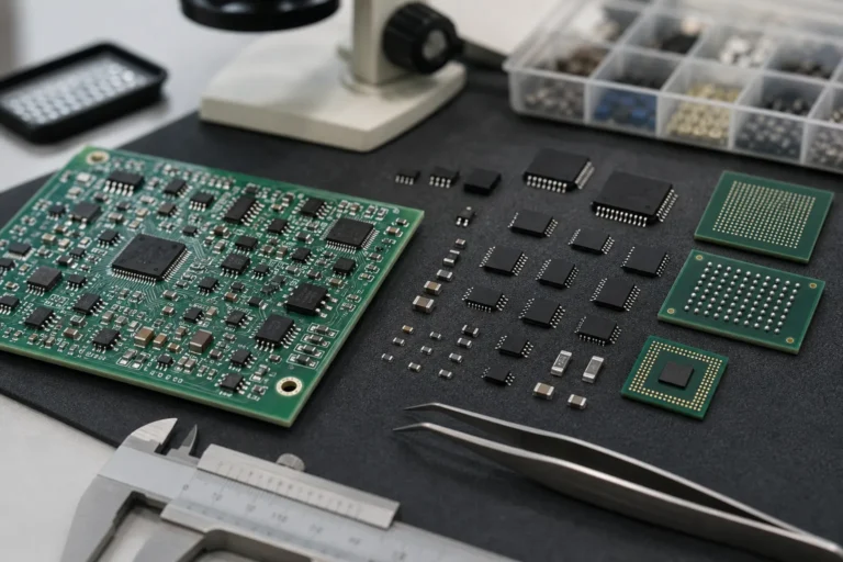
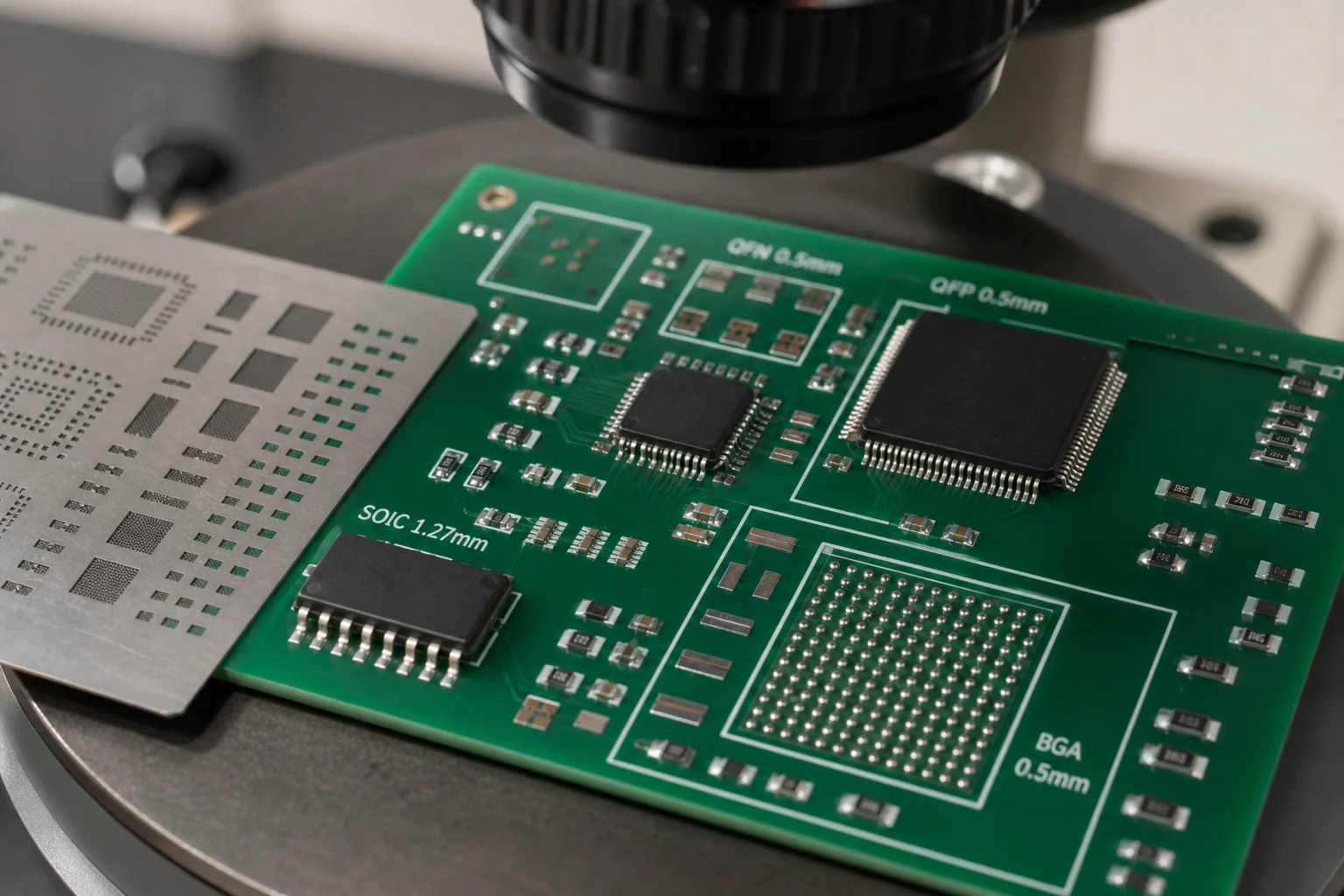
SOIC, TSOP ve QFP paketlerinin görünür beklentileri vardır. Sınavda affederler ve araştırmak veya dokunmak, kurşunsuz paketlemekten daha kolaydır.
QFN ve DFN paketleri yerden tasarruf sağlar ve genellikle termal performansı artırır, ancak pedler gövdenin altında gizlenir. Bu, arazi desenleri disiplini, yapıştırma stratejileri ve termal ped boşaltma kontrolü için risklerini artırır.
BGA paketleri, pin sayısını ve yönlendirme yoğunluğunu en üst düzeye çıkarır, ancak doğrudan görsel denetimler değiştirir. Ürün röntgen erişimini veya dikkatli yeniden çalışma planlamasını haklı çıkaramazsa, BGA yanlış bir kolaylık olabilir.
Pasif çip, boyutu çok agresif hale gelene kadar basit görünüyor. 0603’ten 0201’e yer değiştirme, elektrik tasarımını değiştirmekten çok, yerleştirme kararlılığını, şablon bertarafını ve saha hizmetlerinin pratikliğini değiştirebilir.
Önce boyuta göre seçmek yerine bu seçenek sırasını kullanın
Pratik paket kararları genellikle bu sırayla daha iyi çalışır:
Termal fonksiyon ve yük ile başlayın. Isıya duyarlı güç ve IC cihazları, açık bir yatak veya daha büyük bir bakır arabirimi gerektirebilir.
Yerleştirme ve inceleme yeteneklerini kontrol edin. Yapı ortamı çok ince adımı, ultra küçük pasif veya röntgen doğrulamasını desteklemiyorsa, paketi rastgele seçmeyin.
Yeniden işleme ve hizmetleri düşünün. Biraz daha büyük bir paket, hata ayıklama prototiplerinde, saha iyileştirmelerinde ve mühendislik değişikliği kontrollerinde büyük zaman kazandırabilir.
Ancak o zaman alanı ve maliyeti optimize edin. Pano alanı önemlidir, ancak ürün seviyesinin faydası olmadan süreç penceresini daraltan paketi haklı çıkarmak için yeterli değildir.
Sonucu bozan ortak SMD paket hatası
Termal pede yeterince dikkat etmeden tenekesiz parçanın belirlenmesi. Açık ped, sonradan düşünülen bir şey değil, montaj zorluğunun bir parçasıdır.
Kozmetik nedenlerle mevcut en küçük pasif kullanımı. Küçük paketler, düzenlerin etkileyici ekran görüntülerini onlardan daha fazla gerçek ürünü geliştirir.
erişim denetimini görmezden gelmek. Kritik bağlantı görülemez veya test edilemezse, işlem başka bir yerde telafi edilmelidir.
süreç planlaması olmadan çok farklı paket isteklerini bir panoda karıştırmak. Büyük termal salyangozları, ultra ince perde uçlarını ve pasif 0201’i birleştiren panolar, şablonlar ve kasıtlı profil stratejileri gerektirir.
Hala deliğin daha iyi bir mekanik cevap olup olmadığına karar vermesi gereken bir takım için, Yüzeye monte edilmiş deliğe karşı delikten fedakarlık Bomba yapmadan önce incelemeye değer.
Fabrika tarafından inşa edilebilecek, incelenebilecek ve onarılabilecek bir paket seçin.
En iyi Yüzeye montaj cihazı Nadiren seçenek en küçük, en yeni veya en özlü pakettir. Bu, mantıklı bir üretim penceresinde kalırken elektrik ihtiyaçlarınıza uygun bir pakettir. Mühendisler montaj, inceleme ve onarımı göz önünde bulundurarak paket kararları verdiğinde, panonun başlatılması daha kolay ve üretimde daha güvenilir hale gelir.
Yüzey montaj cihazı nedir?
Yüzey montaj cihazları veya SMD, delinmiş deliklerden geçen kablosuz PCB pedlerine doğrudan lehimlenmek üzere tasarlanmış bileşenlerdir.
SMT ve SMD arasındaki fark nedir?
SMT bir montaj yöntemidir, SMD ise bu yöntem için oluşturulmuş bileşendir. SMD paketini seçersiniz, ardından SMT işlemi ile üretirsiniz.
Paket seçenekleri üretim yeteneklerini neden etkiler?
Paket stili, şablon tasarımını, yerleşim doğruluğunu, muayene erişimini, termal performansı ve yeniden işleme zorluklarını etkiler. Elektriksel olarak eşdeğer iki parça çok farklı montaj riskleri oluşturabilir.
Kurşunsuz paketler her zaman kurşunlu paketlerden daha mı iyidir?
Hayır. Kurşunsuz paketler yerden tasarruf edebilir ve termal davranışı iyileştirebilir, aynı zamanda görsel incelemeye erişimi de azaltabilir ve genellikle yeniden çalışmayı zorlaştırır. En iyi seçim ürüne ve bina ortamına bağlıdır.
Bir mühendis mevcut en küçük pasif boyuttan ne zaman kaçınmalıdır?
Panoların ihtiyaç duymadığı durumlarda veya yerleştirme yetenekleri, yeniden işleme erişimi veya saha hizmeti güvenilirliği, 0201 yerine 0603 gibi biraz daha büyük paketlerle artacaktır.