Apa yang dimaksud SMT dalam perakitan PCB — di luar akronim
post views:14
Daftar Isi
Tanyakan kepada seorang insinyur “Apa itu SMT” dan Anda biasanya akan mendengar “Teknologi Pemasangan Permukaan.” Itu benar. Tetapi jika Anda berhenti di akronim, Anda melewatkan apa SMT sebenarnya berarti Untuk bagaimana PCB dirancang, dibangun, diuji, dan dibayar. Artikel ini menjelaskan tentang Definisi SMT Dalam hal yang penting bagi siapa saja yang merancang, memesan, atau memecahkan masalah papan sirkuit yang dirakit.
Definisi langsung dari SMT
SMT (Teknologi pemasangan permukaan) adalah metode perakitan PCB di mana komponen dipasang langsung ke permukaan papan sirkuit tercetak, tanpa kabel melewati lubang. Ini menggantikan teknologi through-hole (THT) sebagai metode produksi dominan yang dimulai pada 1980-an dan sekarang menyumbang sebagian besar perakitan PCB komersial.
Perbedaan utama: dalam perakitan melalui lubang, lead komponen go melalui lubang yang dibor dan disolder di sisi yang berlawanan. Di SMT, komponen duduk di atas bantalan dicetak dengan pasta solder dan disolder di tempatnya selama reflow. Tidak ada lubang, tidak ada pemangkasan timbal, dan kepadatan komponen yang secara dramatis lebih tinggi.
Perubahan “SMT” tentang desain PCB
Jika Anda tumbuh dengan prototyping melalui lubang, pindah ke SMT berarti memikirkan kembali beberapa kebiasaan desain:
Trace routing gets tighter. SMD pads are smaller and closer together. You can place a decoupling capacitor within a millimeter of an IC power pin, which improves signal integrity in ways through-hole layouts rarely achieve.
Both sides become usable. SMT components can populate both the top and bottom of a board. This doubles the effective area without increasing the PCB outline, which matters a lot in compact consumer products.
Vias become routing tools, not component anchors. Since components don’t need plated through-holes, vias are freed up purely for layer transitions and thermal management.
Thermal design shifts. SMD components dissipate heat into copper planes through their pads rather than through lead wires. A proper copper pour under a power SMD part does more for cooling than a through-hole heatsink clip.
Jika Anda telah menerbitkan desain yang berfokus pada SMT dan ingin memindahkannya ke dalam produksi tanpa mendesain ulang seluruh BOM, Layanan Perakitan ReversePCBS Menangani papan teknologi campuran di mana komponen SMT dan lubang-lubang hidup berdampingan.
SMT vs. Lubang melalui: Realitas Lantai Perakitan
Itu Definisi SMT paling penting di jalur perakitan. Inilah yang berubah ketika sebuah desain beralih dari through-hole ke SMT:
Aspek
melalui lubang
Smt
Penempatan komponen
Perlengkapan manual atau solder gelombang
Pick-and-place otomatis di ribuan CPH
Pematerian
gelombang atau solder tangan
Oven reflow dengan profil termal terkontrol
Dewan Real Estat
Mengkonsumsi kedua sisi dengan lubang timah
Komponen duduk di permukaan, kedua sisi dapat digunakan
Ukuran komponen minimum
~0805 setara
turun ke 01005 (0,4 x 0,2 mm)
kesulitan pengerjaan ulang
Mudah dengan besi solder
Membutuhkan udara panas, pemanasan awal, atau stasiun pengerjaan ulang khusus
kekuatan mekanik
lebih kuat (memimpin melalui lubang)
Lebih lemah terhadap geser, bergantung pada adhesi pad
Untuk sebagian besar produksi berjalan di atas beberapa lusin unit, SMT menang pada kecepatan, konsistensi, dan biaya per unit. Pengorbanannya adalah alat di muka: stensil, pemrograman pick-and-place, dan reflow profiling semuanya terjadi sebelum papan pertama dikirimkan.
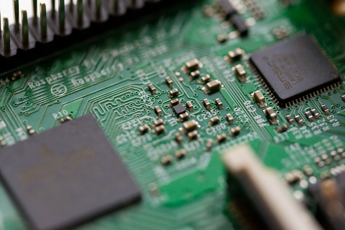
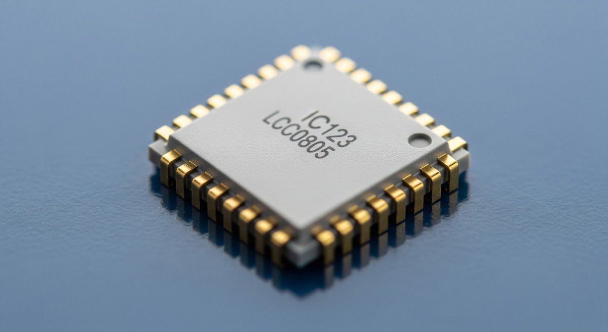
Komponen SMD: Apa yang dipasangPerangkat pemasangan permukaan (SMD) dalam close-up: paket chip, pasif, dan IC mengisi PCB yang padat — setiap jenis komponen mewakili keputusan tentang ukuran paket, kinerja termal, dan kompleksitas perakitan.
Komponen yang digunakan dalam Teknologi pemasangan permukaan disebut SMDS — perangkat pemasangan permukaan. Jenis paket SMD yang umum meliputi:
Passive chips (resistors, capacitors, inductors): Standards like 0402, 0603, 0805. The number is the footprint in hundredths of an inch — an 0603 measures 0.06″ x 0.03″.
SOIC, SSOP, TSSOP: Gull-wing-leaded ICs, the workhorses of analog and mixed-signal circuits.
QFP, LQFP, TQFP: Square ICs with leads on four sides, common on microcontrollers up to ~200 pins.
QFN, DFN: Leadless packages with exposed thermal pads underneath. Harder to hand-solder, excellent thermal performance.
BGA: Ball grid arrays hide solder balls under the package. Impossible to visually inspect after reflow without X-ray.
0201, 01005: Ultra-miniature passives used in phones and wearables. Hand-soldering is not realistic.
Memilih paket yang tepat adalah keputusan manufaktur seperti halnya listrik. Jika produsen kontrak Anda tidak dapat dengan andal menempatkan 0201 suku cadang, jangan tentukan.
Proses perakitan SMT dalam empat langkah
Memahami Teknologi pemasangan permukaan Alur kerja membantu Anda menulis aturan DFM yang lebih baik:
Solder paste printing. A stainless-steel stencil aligns over the bare PCB. Solder paste is squeegeed across it, depositing paste only on component pads. Stencil thickness, aperture design, and paste rheology control the deposit volume.
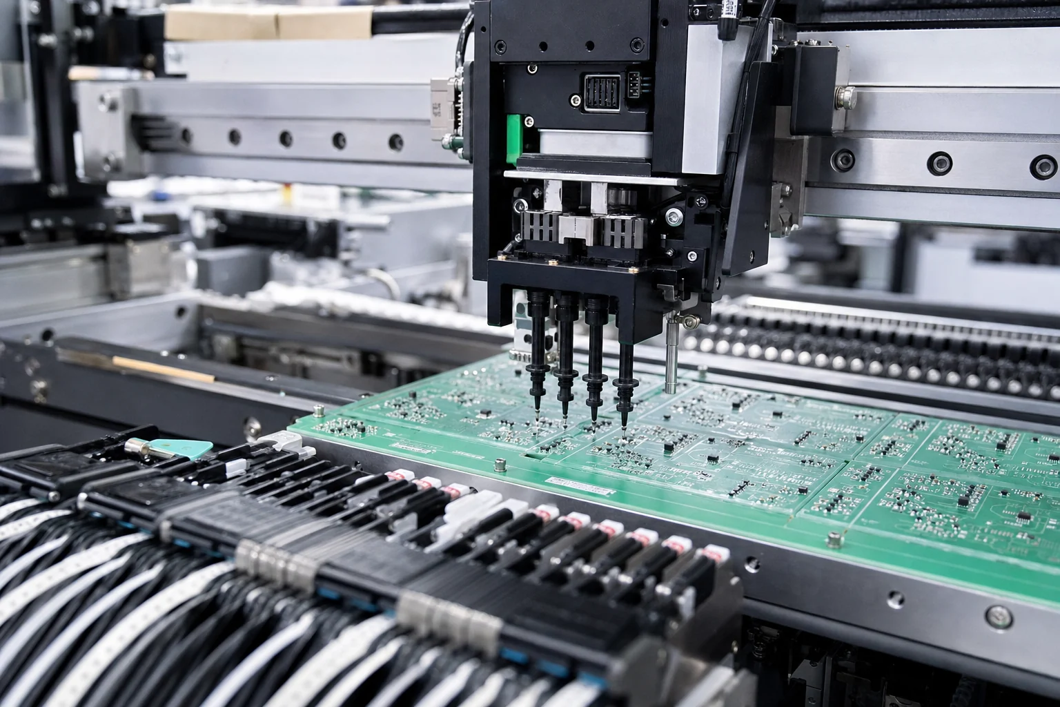
Pick-and-place. A high-speed machine picks SMDs from tape reels or trays using vacuum nozzles and places them onto the pasted pads. Placement accuracy is typically better than 50 µm for modern machines.
Reflow soldering. The populated board travels through a reflow oven with controlled heating zones. The thermal profile ramps up, soaks to activate flux, spikes above liquidus (~217°C for SAC305 lead-free solder), then cools at a controlled rate. The paste melts, wets the pads and component terminations, and solidifies into reliable solder joints.
Inspection. Automated optical inspection (AOI) checks for solder bridges, tombstones, insufficient wetting, and component offsets. Boards with BGAs or hidden joints may also go through X-ray inspection.
Jika Anda merancang papan SMT pertama Anda dan menginginkan mitra manufaktur yang menangkap masalah DFM sebelum membuat prototipe, Ulasan DFM ReversePCBS Tandai stensil, pad, dan masalah penempatan lebih awal.
Cacat SMT Umum dan Apa yang Mereka Katakan kepada Anda
Setiap cacat SMT memiliki akar penyebab. Belajar membacanya membuat Anda lebih cepat dalam memecahkan masalah produksi:
Tombstoning: One end of a chip component lifts off the pad during reflow. Usually caused by uneven heating (one pad reaches liquidus first) or pad geometry imbalance. Fix: equalize pad sizes and thermal relief on both sides.
Solder bridging: Excess solder connects adjacent pads. Common causes: too much paste, stencil aperture too wide, or insufficient spacing between pads.
Insufficient wetting: The solder didn’t form a proper fillet. Check pad oxidation, paste age, or reflow profile — if the board never reached liquidus long enough, wetting fails.
Head-in-pillow: BGA balls and paste melt separately without merging. Usually a reflow profile issue where the package warps and the balls lose contact with paste during the liquid phase.
Voiding: Gas bubbles trapped in the solder joint beneath BGAs or QFNs. Excess flux, moisture, or an aggressive ramp rate can all cause voids.
Aturan desain yang mencegah sakit kepala SMT
Jika Anda mengikuti aturan ini, hasil SMT Anda akan jauh lebih tinggi:
Pad-to-pad spacing: Keep at least 0.2 mm between adjacent pads unless your fab and assembler both approve tighter spacing.
Component-to-edge clearance: Parts within 3 mm of the board edge risk tombstoning from uneven heating near the rail. Move them inward or add thermal relief.
Fiducial marks: Place three global fiducials (one in each corner, asymmetrically) plus local fiducials near fine-pitch parts. Pick-and-place machines use these for optical alignment.
Stencil aperture reduction: For fine-pitch QFPs and 0.5 mm-pitch parts, reduce aperture width by 10–20% to prevent bridging. Your assembler’s stencil engineer should confirm this.
Thermal relief on large copper areas: A pad directly connected to a large ground plane will wick heat away during reflow, causing cold joints. Use thermal relief spokes.
Untuk informasi lebih lanjut tentang disiplin desain-untuk-manufaktur, lihat Panduan DFM ReversePCBS.
ketika smt bukan jawaban yang tepat
SMT mendominasi perakitan PCB, tetapi tidak universal. Through-hole masih menang dalam skenario ini:
Connectors and mechanical stress points. USB ports, barrel jacks, and terminal blocks experience repeated insertion force. Through-hole mounting provides mechanical anchoring that SMT pads cannot match.
High-power components. Large transformers, heat-sinked power transistors, and relay coils often use through-hole for both current capacity and thermal management.
Prototyping and one-off builds. Hand-soldering 0603 passives under a microscope is doable. Hand-soldering a 64-pin QFN is not. Through-hole prototyping remains faster for low-volume work.
Mixed-technology legacy designs. Many industrial and automotive boards combine SMT logic sections with through-hole power and I/O sections. These are fully manufacturable with today’s mixed-technology lines.
Pertanyaan yang sering diajukan
What does SMT stand for?
SMT stands for Surface Mount Technology. It is the PCB assembly method where components mount directly onto the board surface rather than through drilled holes.
What is the difference between SMT and SMD?
SMT refers to the assembly technology (the process). SMD refers to the device (the component itself). An SMD, or surface mount device, is any component designed for SMT assembly.
Why did SMT replace through-hole for most PCB assembly?
SMT enables higher component density, automated high-speed assembly, smaller board sizes, and lower per-unit cost. It also allows components on both board sides, which through-hole cannot match.
Can you mix SMT and through-hole on the same board?
Yes. Mixed-technology boards are common in industrial and automotive electronics. The SMT side is reflowed first, then through-hole components are placed and wave-soldered or hand-soldered.
What is the smallest SMD component size?
01005 (0.4 x 0.2 mm) is the smallest widely-available passive size. These require specialized pick-and-place equipment and are primarily used in smartphones, wearables, and implantable medical devices.
What is the definition of SMT in electronics manufacturing?
In electronics manufacturing, the definition of SMT is an assembly process where solder paste is printed onto PCB pads, components are placed onto the paste by automated equipment, and the entire assembly passes through a reflow oven to form permanent solder joints without through-hole leads.