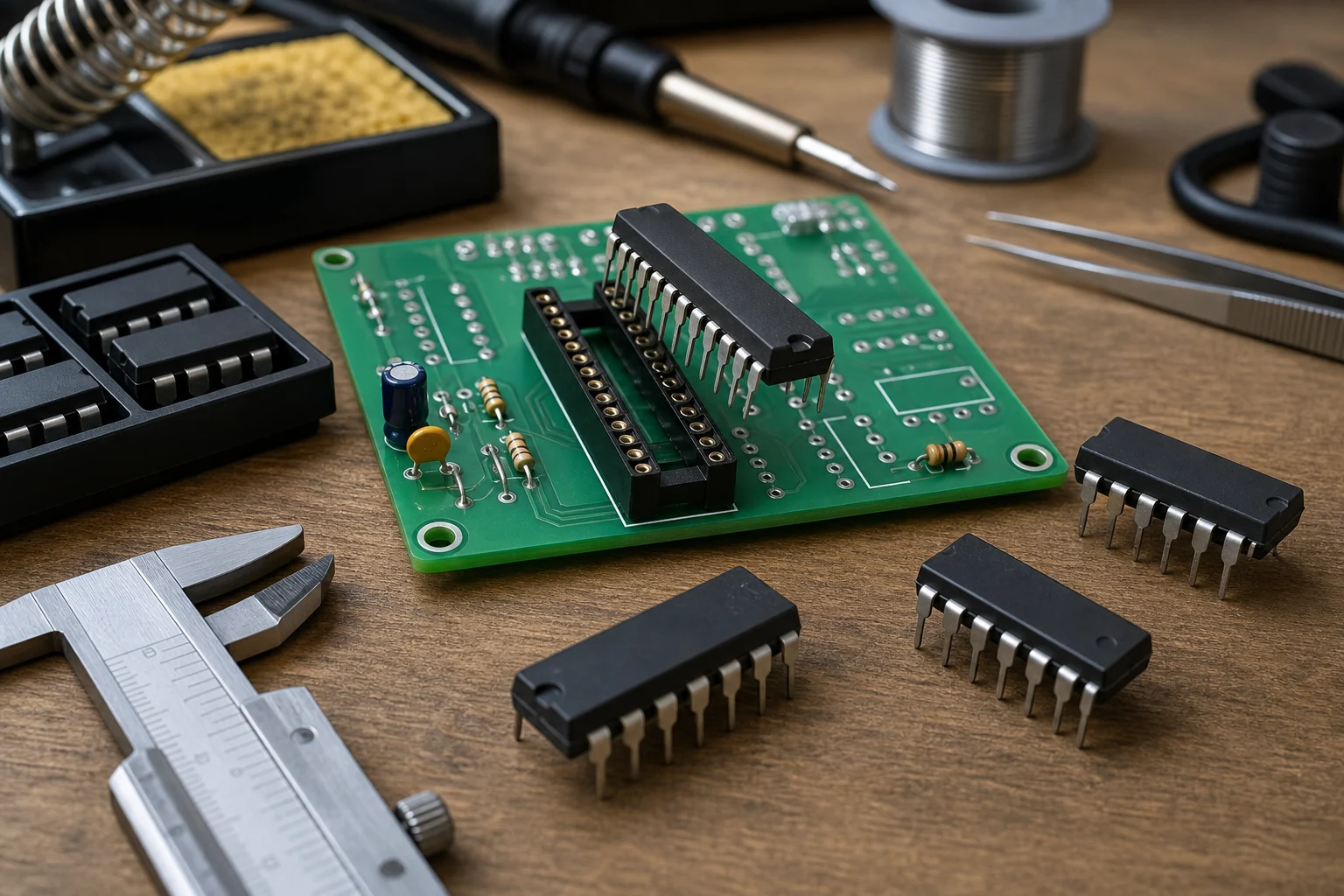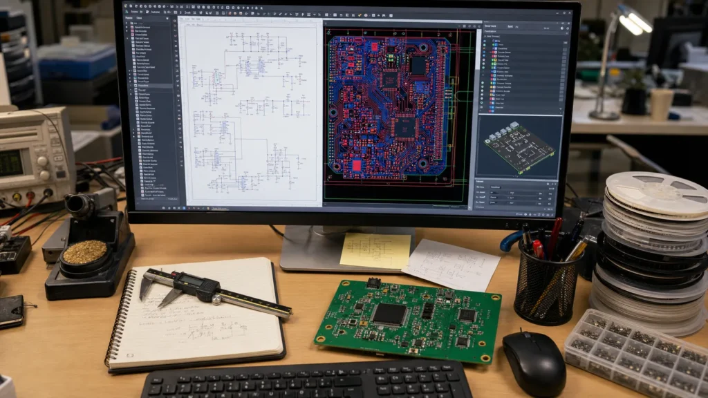
Automação de design eletrônico (EDA) é uma categoria que os engenheiros de software usam para projetar, simular e verificar sistemas eletrônicos antes de criar um único PCB. Procurando por você, pense que “Esquemas de She”, você perderá a maior parte do que a cadeia de ferramentas EDA moderna realmente faz. Este artigo explica como as ferramentas de automação de design eletrônico são diferentesum deOutros e o que eles devem prestar atenção ao escolher uma plataforma EDA para estudos de PCB.
Que coisana verdade está láAutomação de design eletrônico?
pelo menos um Automação de design eletrônico A cadeia de instrumentos elabora quatro etapas:
esquema: desenhe um circuito lógico. É aqui que os símbolos, conexões de cabo e valores de componentes são definidos. Boas ferramentas esquemáticas também são capazes de controlar páginas hierárquicas, regras de design (RDCs) e regras elétricas (ERCs).
Layout de PCB: Converta o esquema na guia física. LO editor de PCB insere impressões digitais, traços de cobre, identifica os níveis deA área e aplique regras de design para permissões, lImpedância e capacidades de produção.
Simulação e análise: Simulação de especiarias para circuito analógico, análise doIntegridade do sinal para análise digital de alta velocidade, simulação térmica e rede de distribuição de energia (PDN). Funciona tudoDentro ou ao lado da ferramenta EDA.
poder de produção: Arquivos Gerber, perfuração de arquivos, coleta e posicionamento de dados e edição de imagens. Os erros nesta fase garantem que a produção seja rejeitada.
Para obter mais informações sobre as práticas recomendadas esquemáticas, consulte. Manual Desenho esquemático do ReversePCBS.
A principal plataforma EDA para o design de PCB
O cenário da EDA é dividido em três níveis e escolher o errado para o seu projeto causa dor real:
| Nível | Veículo | ao melhor | Limitação |
|---|---|---|---|
| Recurso aberto / gratuito | KICAD, EASEYEDA, LIBEPCB | Projeto de hobby, hardware aberto, cartão de 2 a 6 camadas | Simulação avançada limitada, menos poderoso gerenciamento de biblioteca |
| Profissionais de classe média | Altium Designer, OrCAD, Pad | Cartão profissional de 4 a 16 camadas, design de alta velocidade, fluxo de trabalho de ferramentas | Taxa de assinatura, curva de aprendizado íngreme |
| Especialização em Negócios / RF | Cadence Alegre, Mentor Xpedition, AD | Complexo multicamada, RF/Microdal, HDi, Rigi-Flex | Custo muito alto, equipe especial de suporte CAD |
O Kicad preencheu a lacuna com um veículo de médio alcance para muitos projetos. Agora é uma escolha profissional adequada para cartões de até 8 camadas, desde que sua equipe esteja confortável no fluxo de trabalho da biblioteca. Alguns GHz Se você estiver projetando uma placa digital de alta velocidade com memória DDR ou correspondência diferencial, a ferramenta Altium Integrity Tool ou o ritmo das variações de nível se tornam mais difíceis.
Workflow-PCB esquemático emAplicativos
Aqui está a visualização do fluxo de trabalho EDA para um projeto de PCB normal:
Crie um esquema. Coloque símbolos para capturar pinos desconectados ou saídas sobrepostas, malha de arame, definir impressões digitais e LSiga-o.
Crie netlists. NetList é uma lista legível por máquina de cada componente e link. A ferramenta de layout do PCB o importa.
Coloque os componentes. Coloque as impressões digitais no contorno da mesa. Agrupe as peças relevantes, marque corretamente os conectores e abra espaço para os orifícios e áreas de armazenamento.
caminho. Rolando netlists de acordo com E, siga as regras de autorização, requisitos de largura da trilha e objetivos de impedância. As ferramentas modernas de EDA incluem redirecionamento automático, mas as redes críticas sempre devem ser guiadas manualmente.
bem rdcor. O Controlador de Regras de Design verifica se não há vestígios que violam as permissões, que não há links ausentes e que cada rede é completamente redirecionada. O Conselho de Passagem da Rdcil é o requisito mínimo antes de enviar o Conselho para a Produção.
Crie arquivos de produção. Exportar Gerber Drill, NC, arquivos de desenho de bombas e conjuntos. Verifique o visualizador Gerber novamente – lO erro nesta fase é caro.
especialmente oaltiumpcb de etapas esquemáticas para Manual Este passo a passo Passando por um processo completo.
O que deve ser considerado ao escolher as ferramentas EDA?
Concentre-se no que realmente afeta seu projeto, não no número de recursos:
Qualidade e gerenciamento da biblioteca: Esta ferramenta tem faixas verificadas para os componentes que você realmente usa ou passará horas criando símbolos a partir das folhas de dados? Bibliotecas fracas gastam mais tempo do que falta de recursos de simulação.
Capacidade das regras de design: Você pode especificar regras para classe limpa, par diferencial e região? Se você precisa de umImpedância controlada, sua ferramenta calcula a geometria de rastreamento da sua pilha?
Cooperação: Mais de um engenheiro pode trabalhar no mesmo projeto? Ele suporta o controle de versão? LA integração do Git está se tornando cada vez mais padrão em veículos EDA modernos.
Confiabilidade da produção: GerberA exportação corresponde ao papel projetado? Algumas ferramentas aplicam secretamente a correção das regras de design durante oSaídas que mudam as notas. Gerbero Spectator sempre verifica.
Integração de simulação: Se você confiar na simulação do Spice, a ferramenta a integra localmente ou uma netlist Você precisa exportar i para um simulador externo?
Produção e erros comuns
rdcreti que não passam: DRC Se alguns instrumentos estiverem marcados como “sem conexão” permitem que você ignore as redes não diretas. Verifique visualmente cada rede ou um relatório de conexão.
Incompatibilidade dopegada 1: símbolos esquemáticos e traços de PCB não são dAcordo emOrientação do pino 1. Este é o motivo mais comum para a falha do primeiro conselho de revisão. Sempre verifique visualmente oPino 1 em cada monitoramento de IC.
Rolamentos sobrepostos de impressão de tela: impressão de tela impressa em almofadas de cobre evita a soldagem. A maioria das ferramentas possui regras de autorização de pad na impressão da tela – Ativar.
impedância única: Traços de geometria no layout não criam LImpedância de destino, pois eles são identificados incorretamente na ferramenta Stack. Verifique LImpedância com a pilha real do fabricante, não a ferramenta padrão.
Perguntas frequentes
Que coisaé oAutomação de design eletrônico?
Electronic Design Automation (EDA) é uma categoria de software usado para projetar sistemas eletrônicos, incluindo aquisição esquemática, layout de PCB, simulação de circuitos e criação de arquivos de produção. As ferramentas EDA são essenciais para o desenvolvimento moderno de PCB.
O Kicad é bom o suficiente para o design profissional de PCB?
Sim, o Kicad agora é um PCB de nível profissional para placas de até 8 camadas para ter a capacidade de projetar. Suporta roteamento diferencial duplo, ajuste longo e visualização 3D. Ferramentas de Altium ou Rhythm fornecem umaUma análise mais aprofundada para um design de ultra-alta velocidade que requer simulação avançada dointegridade do sinal.
Qual é a diferença entre o layout de aquisição esquemática e o PCB?
O esquema de aquisição é um estágio lógico do projeto no qual a conexão de componentes e funções do circuito é determinada. O layout do PCB é uma fase de design físico em que os componentes são colocados, os sinais de cobre são direcionados e as folhas são preparadas para produção.
Preciso de uma simulação no meu veículo EDA?
A simulação é opcional para um cartão digital simples. Para circuitos analógicos, fonte de alimentação ou design digital de alta velocidade, simulação de especiarias e DellSinalize a integridade, adquira problemas antes da produção e economize voltas de revisão.
Quais arquivos a ferramenta EDA para produção produz?
LA produção padrão de produção inclui arquivos Gerber (formato RS-274X ou X2) para cada camada de cobre, máscara de soldagem e serigrafia; Perfure os arquivos NC; Colete e coloque arquivos (centro) para Lmontagem automática; e faturas materiais (boom).