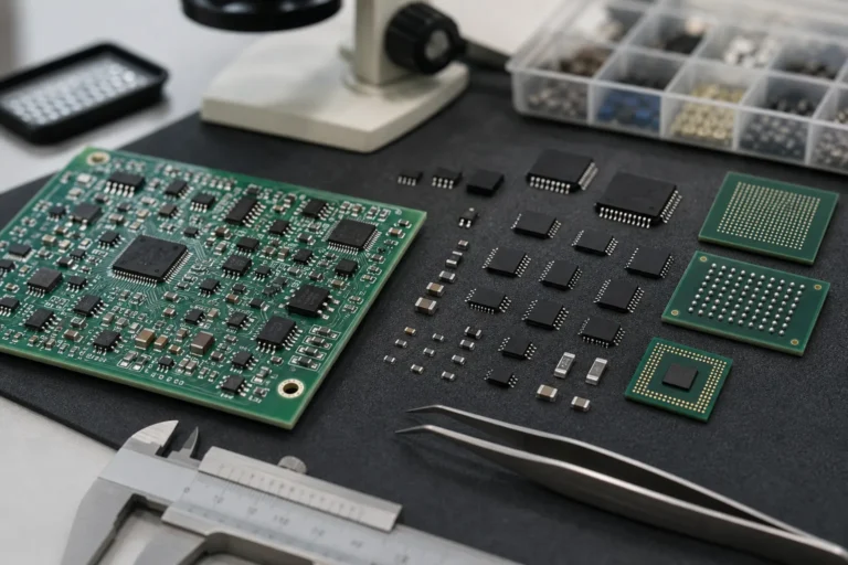
Ля Устройство для поверхностного монтажа это не просто электронная часть, которая помещается на плату. Это решение на производстве. Стиль пакета влияет на высвобождение трафарета, толерантность к размещению, доступ к осмотру, сложность переделки, тепловое поведение и даже то, учит ли пилотная сборка чему-нибудь полезному.
Вот почему выбор SMD-пакетов только по размеру следа только редко бывает достаточно. Инженеры часто оптимизируют стоимость платы или единицы измерения и позже обнаруживают, что реальная штрафная проявляется в настройке фидера, скрытых соединениях или времени ремонта. В этом руководстве рассказывается, как выбирать пакеты для поверхностного монтажа, которые может надежно поддерживать ваш процесс сборки.
Что на самом деле меняет устройство для поверхностного монтажа
Основное определение простое: SMD — это компонент, предназначенный для прямого крепления к поверхностным прокладкам, а не сквозными отверстиями. Но важный инженерный вопрос заключается в том, что этот выбор изменит для сборки.
Плотность доски увеличивается. Меньшие детали и двухсторонняя популяция делают компактные конструкции практичными.
Автоматизация становится по умолчанию. Как только шаг в пакете становится достаточно мелким, предположения о размещении и оплавлении начинают управлять дизайном.
Изменения в проверке Отведения крыла чайки легко осмотреть визуально. Бессвинцовые термальные прокладки и BGA — нет.
Переработка становится зависимой от пакета. Резистор 0603 и тонкий шаг QFN являются SMD, но они не требуют тех же инструментов для ремонта или операторских навыков.
Обратный PCBs Обзор SMT Объясняет сам процесс. Проблема выбора пакета узкая: какой стиль устройства дает вам электрический результат, который вы хотите, не усложняя сборку, чем нужно?
Форма свинца имеет большее значение, чем многие BOMS признают
Выбор пакета часто начинается с лид-системы, потому что лид-система контролирует видимость смачивания, поведение самовыравнивания во время перепрошивки и доступ к доработке.
Пакеты SOIC, TSSOP и QFP имеют видимые лиды. Они прощают в осмотре и легче исследовать или подкрашивать, чем пакеты без свинца.
Пакеты QFN и DFN экономят место и часто улучшают тепловые характеристики, но их колодки прячутся под корпусом. Это повышает ставки на дисциплину наземного шаблона, стратегию пасты и контроль мочеиспускания термальной площадки.
Пакеты BGA максимизируют количество контактов и плотность маршрутизации, но они торгуют прямым визуальным осмотром. Если изделие не может оправдать доступ к рентгеновскому излучению или тщательное планирование переделки, BGA может оказаться неправильным удобством.
Пассивные чипсы кажутся простыми, пока их размер не станет слишком агрессивным. Переход от 06:03 до 0201 может больше изменить устойчивость размещения, высвобождение трафарета и практичность в полевых условиях, чем электрическую конструкцию.
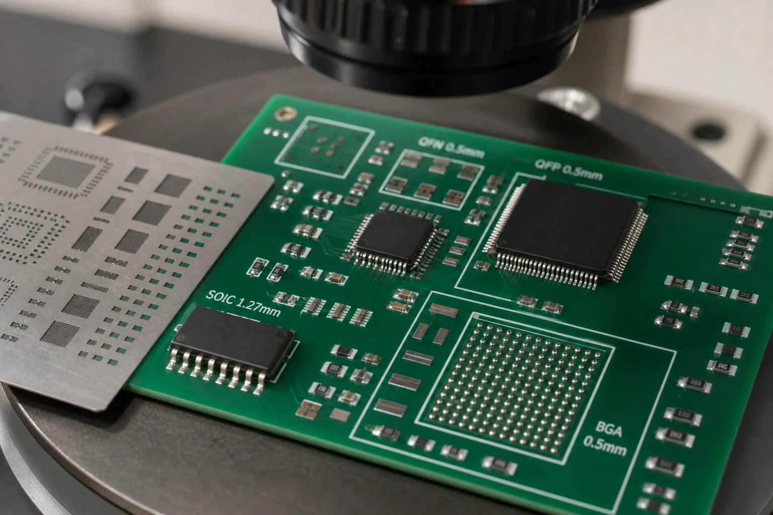
Используйте этот порядок выбора, а не выбирайте сначала по размеру
Практическое решение пакета обычно работает лучше в таком порядке:
Начните с функции и тепловой нагрузки. Силовые устройства и термочувствительные микросхемы могут потребоваться открытые прокладки или более крупные медные интерфейсы.
Проверить возможность размещения и проверки. Если среда сборки не поддерживает очень тонкую подачу, сверхмалую пассивную или рентгеновскую валидацию, не выбирайте эти пакеты небрежно.
Рассмотрим доработку и обслуживание. Немного более крупный пакет может сэкономить значительное время на отладку прототипа, ремонте на местах и управлении инженерными изменениями.
Только тогда оптимизируйте площадь и стоимость. Область правления имеет значение, но недостаточно, чтобы оправдать пакет, который сужает окно процесса без преимущества на уровне продукта.
Распространенные ошибки пакета SMD, которые вредят урожайности
Указание бессвинцовых частей без уделения достаточного внимания термопрокладке. Обнаженная прокладка является частью вызова сборки, а не запоздалой мыслью.
Использование наименьшего пассивного доступного по косметическим причинам. Крошечные пакеты впечатляют скриншот макета больше, чем улучшают многие реальные продукты.
Игнорирование доступа к проверке. Если критический сустав не может быть замечен или испытан, процесс должен компенсироваться в другом месте.
Смешивание совершенно разных требований упаковки на одной доске без планирования процесса. Плата, которая сочетает в себе большие тепловые пробки, сверхтонкие провода и пассивные 0201, нуждается в преднамеренной трафарете и стратегии профиля.
Для команд, которые все еще должны решить, является ли сквозная часть лучшим механическим ответом, Сквозное отверстие и компромиссы Оставайтесь достойными просмотра, прежде чем фиксировать спецификацию.
Выбирайте пакеты, которые фабрика может построить, проверить и отремонтировать
ЛУЧШИЙ Устройство для поверхностного монтажа Выбор редко является самым маленьким, самым новым или самым компактным пакетом. Это упаковка, которая соответствует электрическим потребностям, оставаясь в разумном производстве. Когда инженеры принимают пакетные решения с учетом сборки, осмотра и ремонта, доска становится легче запускать и легче доверять в производстве.
Что такое устройство для поверхностного монтажа?
Устройство для поверхностного монтажа, или SMD, представляет собой компонент, предназначенный для припайки непосредственно к площадкам печатных плат без проходов, проходящих через просверленные отверстия.
В чем разница между SMT и SMD?
SMT — это метод сборки, а SMD — компонент, созданный для этого метода. Вы выбираете пакет SMD, затем производите его с помощью процесса SMT.
Почему выбор пакета влияет на технологичность?
Стиль пакета влияет на дизайн трафарета, точность размещения, доступ к осмотру, тепловые характеристики и сложность доработки. Две электрически эквивалентные детали могут создавать очень разные риски сборки.
Всегда ли бессвинцовые пакеты лучше, чем лидированные пакеты?
Нет. Пакеты без свинца могут экономить пространство и улучшать тепловое поведение, но они также уменьшают доступ к визуальному осмотру и часто усложняют доработку. Лучший выбор зависит от продукта и среды сборки.
Когда инженер должен избегать наименьшего пассивного размера?
Избегайте сверхмалых пассивов, когда плата не нуждается в них или когда возможность размещения, доступ к доработке или надежность полевых работ улучшится с помощью немного большего пакета, такого как 0603 вместо 0201.