Chiedi a un ingegnere “Cos’è SMT” e di solito sentirai “Tecnologia di montaggio a superficie”. è corretto. Ma se ti fermi all’acronimo, ti manca cosa SMT in realtà significa Per come un PCB viene progettato, costruito, testato e pagato. Questo articolo spiega il Definizione di smt In termini che contano per chiunque progetti, ordini o risolvi i circuiti assemblati.
la definizione diretta di SMT
smt (Tecnologia a montaggio superficiale) è un metodo di assemblaggio PCB in cui i componenti vengono montati direttamente sulla superficie di un circuito stampato, senza che i conduttori passino attraverso i fori. Ciò ha sostituito la tecnologia a foro passante (THT) come metodo di produzione dominante a partire dagli anni ’80 e ora rappresenta la stragrande maggioranza dell’assemblaggio di PCB commerciale.
La distinzione chiave: nell’assemblaggio passante, i cavi dei componenti vanno tramite fori praticati e saldati sul lato opposto. In SMT, i componenti si siedono sopra di tamponi stampati con pasta saldante e saldati in posizione durante il riflusso. Nessun buco, nessuna rifilatura del piombo e densità dei componenti notevolmente più elevata.
Cosa cambia “SMT” sulla progettazione di PCB
Se sei cresciuto con la prototipazione a foro passante, passare a SMT significa ripensare diverse abitudini di progettazione:
- L’instradamento della traccia diventa più stretto. I pad SMD sono più piccoli e più vicini tra loro. È possibile posizionare un condensatore di disaccoppiamento entro un millimetro da un pin di alimentazione IC, che migliora l’integrità del segnale in modi che i layout dei fori passanti raramente ottengono.
- Entrambe le parti diventano utilizzabili. I componenti SMT possono popolare sia la parte superiore che inferiore di una scheda. Questo raddoppia l’area efficace senza aumentare lo schema del PCB, che conta molto nei prodotti di consumo compatti.
- I VIA diventano strumenti di instradamento, non ancore componenti. Poiché i componenti non hanno bisogno di fori passanti placcati, i viali vengono liberati esclusivamente per le transizioni degli strati e la gestione termica.
- Cambi di progettazione termica. I componenti SMD dissipano il calore in piani di rame attraverso i loro pad piuttosto che attraverso i fili di piombo. Un corretto versamento di rame sotto una parte di potenza SMD fa di più per il raffreddamento di una clip per dissipatore di foro passante.
Se hai già pubblicato un design incentrato su SMT e vuoi spostarlo in produzione senza riprogettare l’intera distinta base, Servizio di assemblaggio ReversePCBS Gestisce tavole a tecnologia mista in cui coesistono componenti SMT e passanti passanti.
SMT vs. passante: la realtà del pavimento di assemblaggio
Le Definizione di smt conta di più sulla catena di montaggio. Ecco cosa cambia quando un progetto passa da foro passante a SMT:
| Aspetto | foro passante | smt |
|---|---|---|
| Posizionamento dei componenti | Apparecchi manuali o per saldatura a onde | Pick-and-place automatizzato a migliaia di CPH |
| saldatura | saldatura a onda o a mano | Forno Reflow con profilo termico controllato |
| Immobiliare del Consiglio | Consuma entrambi i lati con fori di piombo | I componenti si siedono in superficie, entrambi i lati utilizzabili |
| Dimensione minima del componente | ~0805 Equivalente | fino a 01005 (0,4 x 0,2 mm) |
| Difficoltà di rielaborazione | Facile con saldatore | Richiede aria calda, preriscaldamento o stazione di rilavorazione dedicata |
| Resistenza meccanica | Più forte (foro passante) | Più debole contro il taglio, si basa sull’adesione del pad |
Per la maggior parte delle produzioni al di sopra di una dozzina di unità, SMT vince su velocità, coerenza e costo per unità. Il compromesso è in anticipo: stencil, programmazione pick-and-place e profilazione del riflusso avvengono prima della prima nave da bordo.
Componenti SMD: cosa viene montato
i componenti utilizzati in Tecnologia a montaggio superficiale sono chiamati SMD: dispositivi a montaggio superficiale. I tipi comuni di pacchetti SMD includono:
- Chip passivi (resistori, condensatori, induttori): standard come 0402, 0603, 0805. Il numero è l’impronta in centesimi di pollice – una misura 0603 0,06″ x 0,03″.
- SOIC, SSOP, TSSOP: circuiti integrati guidati da ali di gabbiano, i cavalli di battaglia dei circuiti analogici e a segnale misto.
- QFP, LQFP, TQFP: circuiti integrati con derivazioni su quattro lati, comuni sui microcontrollori fino a ~ 200 pin.
- QFN, DFN: Pacchetti senza piombo con pad termici a vista sotto. Più difficile da saldare a mano, eccellenti prestazioni termiche.
- BGA: Gli array di griglia a palline nascondono le palle di saldatura sotto il pacchetto. Impossibile ispezionare visivamente dopo il riflusso senza raggi X.
- 0201, 01005: passivi ultra-miniatura utilizzati nei telefoni e indossabili. La saldatura a mano non è realistica.
Scegliere il pacchetto giusto è una decisione di produzione tanto quanto uno elettrico. Se il produttore del contratto non può posizionare in modo affidabile 0201 parti, non specificarle.
Il processo di assemblaggio SMT in quattro fasi
capire il Tecnologia a montaggio superficiale Il flusso di lavoro ti aiuta a scrivere regole DFM migliori:
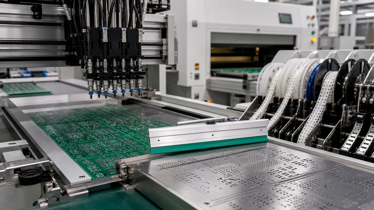
- Stampa in pasta saldante. Uno stencil in acciaio inossidabile si allinea sul PCB nudo. La pasta di saldatura viene schiacciata su di essa, depositando la pasta solo su pad componenti. Lo spessore dello stencil, il design dell’apertura e la reologia incollare controllano il volume del deposito.
- Pick-and-place. Una macchina ad alta velocità preleva SMD da bobine di nastro o vassoi utilizzando ugelli a vuoto e li posiziona sui cuscinetti incollati. La precisione del posizionamento è in genere migliore di 50 µm per le macchine moderne.
- saldatura a riflusso. Il pannello popolato viaggia attraverso un forno a riflusso con zone di riscaldamento controllate. Il profilo termico aumenta, si immerge per attivare il flusso, picchi sopra Liquidus (~217°C per la saldatura senza piombo SAC305), quindi si raffredda a una velocità controllata. La pasta si fonde, bagna le pastiglie e le terminazioni dei componenti e si solidifica in giunti saldatori affidabili.
- ispezione. Ispezione ottica automatizzata (AOI) verifica per ponti di saldatura, lapidi, bagnatura insufficiente e offset dei componenti. Le tavole con BGA o articolazioni nascoste possono anche passare attraverso l’ispezione a raggi X.
Se stai progettando la tua prima scheda SMT e desideri un partner di produzione che solleciti i problemi di DFM prima di prototipare, Revisione DFM ReversePCBS Segnala i problemi di stencil, pad e posizionamento in anticipo.
Difetti SMT comuni e cosa ti dicono
Ogni difetto SMT ha una causa principale. Imparare a leggerli ti rende più veloce nella risoluzione dei problemi di produzione:
- Lapide: un’estremità di un componente di chip solleva il pad durante il riflusso. Di solito causato da riscaldamento irregolare (un pad raggiunge prima Liquidus) o squilibrio geometrico del pad. FIX: equalizzare le dimensioni dei tamponi e il rilievo termico su entrambi i lati.
- Ponte di saldatura: la saldatura in eccesso collega i pad adiacenti. Cause comuni: troppa pasta, apertura stencil troppo ampia o spaziatura insufficiente tra i cuscinetti.
- Bagnatura insufficiente: la saldatura non formava un filetto adeguato. Controllare l’ossidazione del tampone, l’età della pasta o il profilo di riflusso: se la tavola non ha mai raggiunto Liquidus abbastanza a lungo, la bagnatura fallisce.
- Testa in cuscino: le palline BGA e la pasta si sciolgono separatamente senza fondersi. Di solito un problema di profilo di riflusso in cui il pacco si deforma e le palle perdono il contatto con la pasta durante la fase liquida.
- Svuotamento: bolle di gas intrappolate nel giunto di saldatura sotto BGA o QFN. Il flusso in eccesso, l’umidità o una velocità di rampa aggressiva possono causare vuoti.
Regole di progettazione che prevengono il mal di testa SMT
Se segui queste regole, la tua resa SMT sarà misurabilmente più alta:
- Spaziatura pad-to-pad: mantenere almeno 0,2 mm tra i pad adiacenti a meno che il vostro favoloso e l’assemblatore non approvino entrambi una spaziatura più stretta.
- Gioco da componente a bordo: parti entro 3 mm dal bordo del bordo Rischio lapidi da riscaldamento irregolare vicino alla rotaia. Spostali verso l’interno o aggiungi rilievo termico.
- Segni fiduciali: posizionare tre fiduciali globali (uno in ogni angolo, asimmetrico) più fiduciali locali vicino a parti a passo fine. Le macchine pick-and-place li utilizzano per l’allineamento ottico.
- Riduzione dell’apertura dello stencil: per QFP a passo fine e parti di passo di 0,5 mm, ridurre la larghezza dell’apertura del 10–20% per prevenire il bridging. L’ingegnere stencil del tuo assemblatore dovrebbe confermarlo.
- Rilievo termico su grandi aree di rame: un pad direttamente collegato a un grande piano di terra espellerà il calore durante il riflusso, causando giunti freddi. Utilizzare i raggi di sollievo termico.
Per ulteriori informazioni sulla disciplina di design per la produzione, vedere ReversePCBS Guida DFM.
Quando SMT non è la risposta giusta
SMT domina l’assieme PCB, ma non è universale. Through-Hole vince ancora in questi scenari:
- Connettori e punti di sollecitazione meccanici. Porte USB, jack a barilotto e morsettiere subiscono una forza di inserimento ripetuta. Il montaggio a foro passante fornisce un ancoraggio meccanico che i pad SMT non possono eguagliare.
- Componenti ad alta potenza. Trasformatori di grandi dimensioni, transistor di potenza dissipati e bobine a relè spesso utilizzano foro passante sia per la capacità di corrente che per la gestione termica.
- Prototipazione e build una tantum. La saldatura a mano 0603 passivi al microscopio è fattibile. La saldatura a mano di un QFN a 64 pin non lo è. La prototipazione a foro passante rimane più veloce per il lavoro a basso volume.
- Disegni legacy di tecnologia mista. Molte schede industriali e automobilistiche combinano sezioni logiche SMT con potenze passanti e sezioni di I/O. Questi sono completamente producibili con le linee di tecnologia mista di oggi.
Domande frequenti
Cosa significa SMT?
SMT sta per Surface Mount Technology. È il metodo di assemblaggio del PCB in cui i componenti si montano direttamente sulla superficie della scheda piuttosto che attraverso i fori praticati.
Qual è la differenza tra SMT e SMD?
SMT si riferisce alla tecnologia di assemblaggio (il processo). SMD si riferisce al dispositivo (il componente stesso). Un SMD, o dispositivo a montaggio superficiale, è qualsiasi componente progettato per l’assemblaggio SMT.
Perché SMT ha sostituito il foro passante per la maggior parte dell’assemblaggio di PCB?
SMT consente una maggiore densità dei componenti, un assemblaggio automatizzato ad alta velocità, dimensioni di schede inferiori e costi per unità inferiori. Permette anche componenti su entrambi i lati della tavola, che non possono eguagliare.
Puoi mescolare SMT e passante sulla stessa scheda?
si. I tavole a tecnologia mista sono comuni nell’elettronica industriale e automobilistica. Il lato SMT viene prima riflusso, quindi i componenti del foro passante vengono posizionati e saldati a onda o saldati a mano.
Qual è la dimensione del componente SMD più piccola?
01005 (0,4 x 0,2 mm) è la più piccola dimensione passiva ampiamente disponibile. Questi richiedono apparecchiature pick-and-place specializzate e vengono utilizzate principalmente in smartphone, dispositivi indossabili e dispositivi medici impiantabili.
Qual è la definizione di SMT nella produzione elettronica?
Nella produzione elettronica, la definizione di SMT è un processo di assemblaggio in cui la pasta di saldatura viene stampata su pad PCB, i componenti vengono posizionati sulla pasta da apparecchiature automatizzate e l’intero assemblaggio passa attraverso un forno a riflusso per formare giunti saldanti permanenti senza cavi passanti.