1. Pilih Tipe Jalur (Trace)
2. Masukkan Parameter
mils
mils
mils
mils
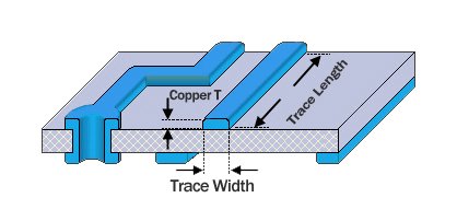
Diagram Microstrip
Rumus
Diagram Stripline
Rumus
Diagram Coupled Microstrip
Rumus
Diagram Coupled Stripline
Rumus
3. Hasil Kalkulasi
Impedansi Karakteristik (Zo)-- Ω
Impedansi Diferensial (Zdiff)-- Ω
Penafian: Kalkulasi ini hanya untuk tujuan estimasi. Untuk desain akhir, selalu gunakan perangkat lunak simulasi profesional.
Panduan Penggunaan
- Pilih Jenis
Jalur Pilih salah satu dari empat konfigurasi jalur dengan ikon visual:- Microstrip: Jalur tunggal pada lapisan luar di atas bidang ground.
- Stripline: Jalur tertanam di antara dua bidang ground.
- Microstrip Terhubung Tepi: Pasangan diferensial pada lapisan luar.
- Stripline Terhubung Tepi: Pasangan diferensial tertanam di antara bidang ground.
- Masukkan Parameter
- Konstanta Dielektrik (εr): Permittivitas listrik bahan (misalnya, 4,4 untuk FR-4).
- Ketebalan Jalur (T): Ketebalan tembaga dalam mil (1 oz = 1,37 mil).
- Lebar Jalur (W): Lebar konduktor dalam mil.
- Tinggi Substrat (H)/Jarak Antar-Plane (B): Jarak ke plane ground.
- Jarak Jalur (S): Muncul untuk pasangan diferensial; jarak antar jalur.
- Lihat Hasil
- Impedansi Karakteristik (Zo): Untuk jalur tunggal.
- Impedansi Diferensial (Zdiff): Untuk pasangan terhubung, ditampilkan secara otomatis untuk tipe terhubung tepi.
Penjelasan Rumus
Impedansi Microstrip Ujung Tunggal
Variables:
- Z0: Characteristic impedance of the microstrip line (Ω)
- Key parameter for single-ended signal integrity
- Typical target: 50Ω for RF, 60-70Ω for digital signals
- εr: Substrate dielectric constant
- FR-4: 4.2-4.6 @ 1MHz
- Rogers RO3003: 3.0 @ 10GHz
- H: Substrate height from trace to ground plane (mils)
- Also known as dielectric height
- Thinner H increases Z0 for same trace width
- W: Trace width (mils)
- Wider traces lower Z0 linearly
- Minimum width limited by manufacturing (typically ≥4mils)
- T: Trace thickness (mils)
- 1oz copper: 1.37mils (35μm)
- 2oz copper: 2.74mils (70μm)
Impedansi Jalur Simetris
Variables:
- Z0: Characteristic impedance of stripline (Ω)
- Enclosed between two ground planes for better shielding
- Typical target: 50Ω for controlled impedance designs
- εr: Dielectric constant of core material
- High-frequency materials: εr stability critical
- Example: Isola FR408HR: εr=3.48 @ 10GHz
- B: Total distance between ground planes (mils)
- Also called "plane separation" or "stackup height"
- B = 2H for symmetric stripline with centered trace
- W: Trace width (mils)
- Narrower W increases Z0 in stripline designs
- Width-to-thickness ratio affects field distribution
- T: Trace thickness (mils)
- Thicker traces reduce DC resistance but impact Z0 slightly
- Considered in denominator for geometric correction
Impedansi Diferensial Microstrip yang Terhubung Tepi
Variables:
- Zdiff: Differential impedance of coupled microstrip (Ω)
- Typical targets: 100Ω (USB), 90Ω (Ethernet)
- Depends on both single-ended Z0 and coupling factor
- Z0: Single-ended microstrip impedance (Ω)
- Base impedance of each trace in the pair
- Assumes infinite ground plane for isolation
- S: Spacing between coupled traces (mils)
- Critical for crosstalk and differential impedance control
- S/H ratio determines exponential coupling factor
- Common rule: S ≥ 2W for minimal crosstalk
- H: Substrate height (mils)
- Affects field penetration into substrate
- Lower H increases electromagnetic coupling between traces
Impedansi Diferensial Jalur Garis yang Terhubung Tepi
Variables:
- Zdiff: Differential impedance of coupled stripline (Ω)
- Preferred for high-speed signals requiring low EMI
- Typical value: 100Ω for DDR4 differential pairs
- Z0: Single-ended stripline impedance (Ω)
- Impedance of each trace when isolated
- Calculated using symmetric stripline formula
- S: Spacing between coupled traces (mils)
- Smaller S increases differential impedance due to coupling
- Exponential term: e-1.5S/B models field overlap
- B: Plane separation (mils)
- Total distance between top and bottom ground planes
- B = 2H for centered traces in symmetric stackups
- Larger B reduces coupling effect for same trace spacing
Pertanyaan yang Sering Diajukan
Apa itu impedansi karakteristik (Z0)?
Characteristic impedance is the resistance a signal "sees" as it travels along a transmission line, determined by trace geometry and material properties. A mismatch in Z0 causes signal reflections, degrading integrity. For example, a microstrip with W = 10 mils, H = 6 mils, and εr = 4.4 has:
Z0 =
87
√
(εr + 1.41)
· ln(
5.98 · H
0.8 · W + T
) ≈ 50 Ω
Apa perbedaan antara microstrip dan stripline?
- Microstrip: Single trace on the surface with a ground plane below.
- Advantages: Easy to route, suitable for low-frequency designs.
- Disadvantages: Radiates EMI, sensitive to board flexing.
- Stripline: Trace sandwiched between two ground planes.
- Advantages: Better EMI shielding, stable at high frequencies.
- Disadvantages: Requires inner layers, more complex to route.
Bagaimana jarak jejak memengaruhi impedansi diferensial?
In edge-coupled pairs, increased spacing S reduces electromagnetic coupling, increasing differential impedance Zdiff. For microstrips:
Zdiff = 2 · Z0 · (1 − 0.347 · e−2.9S/H)
- When S = H: Zdiff ≈ 2Z0 · 0.76
- When S = 3H: Zdiff ≈ 2Z0 · 0.97
Apa perbedaan antara impedansi single-ended dan impedansi diferensial?
| Parameter | Single-Ended (Z0) | Differential (Zdiff) |
|---|---|---|
| Definition | Impedance from trace to ground | Impedance between two coupled traces |
| Typical Values | 50Ω (RF), 60-70Ω (digital) | 100Ω (USB), 90Ω (Ethernet) |
| Application | Single-ended signals (e.g., GPIO) | Differential signals (e.g., LVDS, PCIe) |
| Design Focus | Trace width and ground plane distance | Trace spacing and coupling coefficient |
Differential pairs offer better noise immunity because the differential signal cancels common-mode noise. For example, USB 3.0 requires with and on a 6-mil FR-4 substrate.
Mengapa memilih Microstrip Terhubung Tepi daripada Stripline untuk pasangan diferensial?
- Microstrip: Lebih mudah untuk dirutekan, tetapi memancarkan EMI dan sensitif terhadap tekukan papan.
- Stripline: Pelindung yang lebih baik, gangguan silang yang lebih sedikit, dan lebih stabil pada frekuensi tinggi, tetapi memerlukan lapisan dalam.
Peran apa yang dimainkan oleh konstanta dielektrik (εr) dalam impedansi?
A higher εr increases the effective permittivity of the transmission line, decreasing Z0. For example:
- FR-4 (εr = 4.4): Z0 ≈ 50 Ω for W = 10 mils, H = 6 mils
- Rogers RO3003 (εr = 3.0): Z0 ≈ 58 Ω for the same geometry
Key Dielectric Properties
- εr: Relative permittivity, affects field confinement.
- High-frequency materials: εr stability is critical
- Example: Isola FR408HR: εr = 3.48 @ 10GHz
- Loss Tangent (Df): Energy loss factor, impacts signal attenuation.
- FR-4: Df ≈ 0.02 @ 1MHz
- Rogers RO4350B: Df = 0.004 @ 10GHz
Seberapa akurat perhitungan-perhitungan ini?
Results are based on IPC-standard approximations. Real-world factors like:
- Trace roughness (e.g., 2.1μm RMS)
- Solder mask thickness (0.5-1.0mils)
- Manufacturing tolerances (±10% for trace width)
- Dielectric thickness variation (±5%)