Pergunte a um engenheiro “o que é SMT” e você geralmente ouvirá “tecnologia de montagem em superfície”. Isso mesmo. Mas se você parar na sigla, você perde o que SMT realmente significa Para saber como um PCB é projetado, construído, testado e pago. Este artigo explica a Definição de SMT Em termos que importam para qualquer pessoa que projete, ordens ou solucione problemas montadas em placas de circuito.
A definição direta de SMT
SMT (Tecnologia de montagem em superfície) é um método de montagem de PCB, onde os componentes são montados diretamente na superfície de uma placa de circuito impresso, sem que os cabos passem por orifícios. Isso substituiu a tecnologia através de furos (THT) como o método de produção dominante a partir da década de 1980 e agora representa a grande maioria dos conjuntos de PCBs comerciais.
A distinção fundamental: na montagem de orifícios, os leads dos componentes vão através Perfurou os furos e soldado no lado oposto. Em SMT, os componentes sentam-se no topo de almofadas impressas com pasta de solda e são soldadas no lugar durante o refluxo. Sem orifícios, sem corte de chumbo e densidade de componentes dramaticamente mais alta.
O que muda “SMT” no design de PCB
Se você cresceu em uma prototipagem de orifícios, mudar para SMT significa repensar vários hábitos de design:
- O roteamento de rastreamento fica mais rígido. As almofadas SMD são menores e mais próximas. Você pode colocar um capacitor de desacoplamento dentro de um milímetro de um pino de alimentação IC, o que melhora a integridade do sinal de maneiras que os layouts de orifício raramente alcançam.
- Ambos os lados se tornam utilizáveis. Os componentes SMT podem preencher a parte superior e inferior de uma placa. Isso dobra a área eficaz sem aumentar o contorno do PCB, o que importa muito em produtos de consumo compactos.
- As vias se tornam ferramentas de roteamento, não âncoras de componentes. Como os componentes não precisam de orifícios de passagem chapeados, as vias são liberadas exclusivamente para transições de camadas e gerenciamento térmico.
- Mudanças de design térmico. Os componentes SMD dissipam o calor em planos de cobre através de suas almofadas e não através de fios de chumbo. Um despejo de cobre adequado sob uma peça de energia SMD faz mais para resfriamento do que um clipe de dissipador de orifício.
Se você já publicou um design focado em SMT e quer transferi-lo para a produção sem redesenhar toda a BOM, Serviço de montagem do ReversePCBS Lida com placas de tecnologia mista onde os componentes SMT e orifícios de passagem coexistem.
SMT vs. Through-Hole: The Assembly Floor Reality
Os Definição de SMT Importa mais na linha de montagem. Aqui está o que muda quando um design muda de um buraco para SMT:
| Aspecto | orifício de passagem | sm |
|---|---|---|
| Colocação de componentes | acessórios manuais ou de solda | Pick-and-place automatizado em milhares de CPH |
| De solda | Solda de onda ou mão | Forno de refluxo com perfil térmico controlado |
| Imóveis da diretoria | Consome ambos os lados com orifícios de chumbo | Os componentes ficam na superfície, ambos os lados utilizáveis |
| Tamanho mínimo do componente | ~0805 equivalente | até 01005 (0,4 x 0,2 mm) |
| Dificuldade de retrabalho | Fácil com um ferro de solda | Requer ar quente, pré-aquecimento ou estação de retrabalho dedicada |
| resistência mecânica | Mais forte (buraco de chumbo) | Mais fraco contra o cisalhamento, depende da adesão da almofada |
Para a maioria das execuções de produção acima de algumas dezenas de unidades, o SMT vence em velocidade, consistência e custo por unidade. A compensação é uma ferramenta inicial: estêncil, programação de pick-and-place e perfis de refluxo acontecem antes do primeiro navio ser enviado.
Componentes SMD: o que é montado
Os componentes usados em Tecnologia de montagem em superfície são chamados de SMDs — dispositivos de montagem em superfície. Os tipos comuns de pacotes SMD incluem:
- Chips passivos (resistores, capacitores, indutores): padrões como 0402, 0603, 0805. 0,03″.
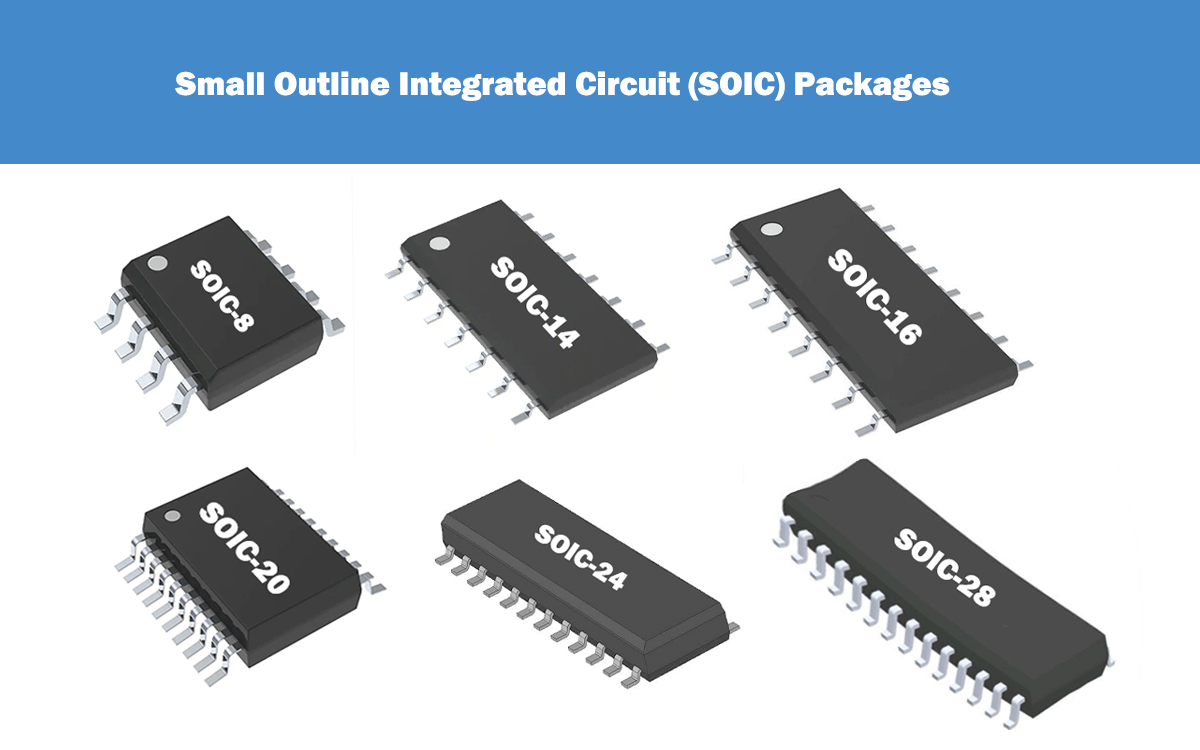
- SOIC, SSOP, TSSOP: ICS com chumbo de gaivota, os cavalos de batalha de circuitos de sinal analógico e misto.
- QFP, LQFP, TQFP: Quadrado de ICS com cabos em quatro lados, comuns em microcontroladores de até 200 pinos.
- QFN, DFN: pacotes sem chumbo com almofadas térmicas expostas por baixo. Mais difícil de soldar à mão, excelente desempenho térmico.
- BGA: Os arranjos de grade de bola escondem bolas de solda sob o pacote. Impossível inspecionar visualmente após o refluxo sem raios-x.
- 0201, 01005: Passivas ultra-miniatura usadas em telefones e wearables. A solda manual não é realista.
Escolher o pacote certo é uma decisão de fabricação tanto quanto elétrica. Se o fabricante do seu contrato não puder colocar 0201 peças de forma confiável, não as especifique.
O processo de montagem SMT em quatro etapas
Entendendo o Tecnologia de montagem em superfície O fluxo de trabalho ajuda você a escrever melhores regras de DFM:
- Impressão em pasta de solda. Um estêncil de aço inoxidável se alinha sobre o PCB nu. A pasta de solda é espremida, depositando pasta apenas nas almofadas dos componentes. A espessura do estêncil, o design da abertura e a reologia da pasta controlam o volume do depósito.
- Pick-and-Place. Uma máquina de alta velocidade escolhe SMDs de carretéis ou bandejas usando bicos de vácuo e os coloca sobre as almofadas coladas. Normalmente, a precisão do posicionamento é melhor do que 50 µm para máquinas modernas.
- Solda de refluxo. A prancha povoada viaja através de um forno de refluxo com zonas de aquecimento controladas. O perfil térmico aumenta, mergulha para ativar o fluxo, fica acima do Liquidus (~217°C para solda sem chumbo SAC305), e então esfria a uma taxa controlada. A pasta derrete, molha as pastilhas e terminações dos componentes e se solidifica em juntas de solda confiáveis.
- inspeção. A inspeção óptica automatizada (AOI) verifica as pontes de solda, lápides, umedecimento insuficiente e deslocamentos de componentes. Placas com BGAs ou juntas escondidas também podem passar por uma inspeção de raios X.
Se você está projetando sua primeira placa SMT e deseja um parceiro de fabricação que detecta problemas de DFM antes da prototipagem, Revisão do DFM ReversePCBS Sinalizadores de estêncil, bloco e problemas de posicionamento antecipadamente.
Defeitos comuns de SMT e o que eles dizem
Cada defeito SMT tem uma causa raiz. Aprender a lê-los torna você mais rápido na solução de problemas de produção:
- Tombstone: uma extremidade de um componente de chip levanta a almofada durante o refluxo. Geralmente causado por aquecimento desigual (uma almofada atinge o Liquidus primeiro) ou desequilíbrio da geometria da almofada. CORREÇÃO: Equalize os tamanhos das almofadas e o alívio térmico em ambos os lados.
- Ponte de solda: o excesso de solda conecta as pastilhas adjacentes. Causas comuns: muita pasta, abertura de estêncil muito ampla ou espaçamento insuficiente entre as almofadas.
- Umedecimento insuficiente: a solda não formou um filete adequado. Verifique a oxidação da almofada, a idade da pasta ou o perfil de refluxo — se a placa nunca atingiu o Liquidus por tempo suficiente, a molhar falha.
- Head-in-Pillow: as bolas BGA e a pasta derretem separadamente sem se fundirem. Normalmente, um problema de perfil de refluxo onde o pacote se deforma e as bolas perdem o contato com a pasta durante a fase líquida.
- Equipamento: bolhas de gás presas na junta de solda sob BGAs ou QFNs. O excesso de fluxo, umidade ou uma taxa de rampa agressiva podem causar vazios.
Regras de design que evitam dores de cabeça SMT
Se você seguir essas regras, seu rendimento SMT será mensuravelmente maior:
- Espaçamento entre almofadas: mantenha pelo menos 0,2 mm entre as almofadas adjacentes, a menos que seu fab e o montador aprovem um espaçamento mais apertado.
- Folga do componente a borda: Peças a 3 mm do risco da borda da placa, se tornando o aquecimento irregular próximo ao trilho. Mova-os para dentro ou adicione alívio térmico.
- Marcas fiduciais: coloque três fiduciais globais (um em cada canto, assimetricamente) mais fiduciais locais perto de peças de passo fino. As máquinas de escolher e colocar usam-nas para o alinhamento óptico.
- Redução da abertura do estêncil: para QFPs de passo fino e peças de passo de 0,5 mm, reduza a largura da abertura em 10 a 20% para evitar a ponte. O engenheiro de estêncil do seu montador deve confirmar isso.
- Alívio térmico em grandes áreas de cobre: uma almofada conectada diretamente a um grande plano de aterramento irá absorver o calor durante o refluxo, causando juntas frias. Use raios térmicos.
Para saber mais sobre a disciplina de design para manufatura, consulte Guia DFM ReversePCBS.
quando smt não é a resposta certa
O SMT domina a montagem do PCB, mas não é universal. A passagem ainda vence nestes cenários:
- Conectores e pontos de tensão mecânica. Portas USB, tomadas de barril e blocos de terminais têm força de inserção repetida. A montagem através do orifício fornece ancoragem mecânica que as almofadas SMT não combinam.
- Componentes de alta potência. Grandes transformadores, transistores de potência afundados e bobinas de relé geralmente usam o orifício de passagem tanto para a capacidade de corrente quanto para o gerenciamento térmico.
- Prototipagem e builds únicos. Solda 0603 passivas sob um microscópio é factível. Solda manual de um QFN de 64 pinos não é. A prototipagem por meio de orifícios de passagem permanece mais rápida para trabalhos de baixo volume.
- Projetos legados de tecnologia mista. Muitas placas industriais e automotivas combinam seções de lógica SMT com seções de potência e E/S. Estes são totalmente fabrisáveis com as linhas de tecnologia mista de hoje.
Perguntas frequentes
O que significa SMT?
SMT significa tecnologia de montagem em superfície. É o método de montagem da PCB, onde os componentes são montados diretamente na superfície da placa e não através de furos.
Qual é a diferença entre SMT e SMD?
SMT refere-se à tecnologia de montagem (o processo). SMD refere-se ao dispositivo (o componente em si). Um SMD, ou dispositivo de montagem em superfície, é qualquer componente projetado para montagem SMT.
Por que o SMT substituiu o orifício de passagem para a maioria dos conjuntos de PCB?
O SMT permite uma densidade de componentes mais alta, uma montagem automatizada de alta velocidade, um tamanho de placa menor e um custo por unidade inferior. Ele também permite componentes em ambos os lados da placa, que não podem igualar.
Você pode misturar SMT e orifícios na mesma placa?
Sim. Placas de tecnologia mista são comuns em eletrônicos industriais e automotivos. O lado SMT é refluído primeiro e, em seguida, os componentes do orifício são colocados e soldados por ondas ou soldados à mão.
Qual é o menor tamanho de componente SMD?
01005 (0,4 x 0,2 mm) é o menor tamanho passivo amplamente disponível. Eles exigem equipamentos especializados de pick-and-place e são usados principalmente em smartphones, wearables e dispositivos médicos implantáveis.
Qual é a definição de SMT na fabricação de eletrônicos?
Na fabricação de eletrônicos, a definição de SMT é um processo de montagem em que a pasta de solda é impressa nas almofadas de PCB, os componentes são colocados na pasta por equipamentos automatizados e todo o conjunto passa por um forno de refluxo para formar juntas de solda permanentes sem cabos de passagem.